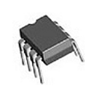
LMC662CN National Semiconductor, LMC662CN Datasheet - Page 4

LMC662CN
Manufacturer Part Number
LMC662CN
Description
Operational Amplifier (Op-Amp) IC
Manufacturer
National Semiconductor
Type
General Purpose Amplifierr
Datasheet
1.LMC662CN.pdf
(14 pages)
Specifications of LMC662CN
No. Of Amplifiers
2
Slew Rate
1.1V/µs
No. Of Pins
8
Peak Reflow Compatible (260 C)
No
Leaded Process Compatible
No
Mounting Type
Through Hole
Package / Case
8-DIP
Rail/rail I/o Type
Rail to Rail Output
Number Of Elements
2
Unity Gain Bandwidth Product
1.4MHz
Common Mode Rejection Ratio
63dB
Input Offset Voltage
6mV
Input Bias Current
2fA
Single Supply Voltage (typ)
5/9/12/15V
Dual Supply Voltage (typ)
Not RequiredV
Voltage Gain In Db
126.02dB
Power Supply Rejection Ratio
63dB
Power Supply Requirement
Single
Shut Down Feature
No
Single Supply Voltage (min)
4.75V
Single Supply Voltage (max)
15.5V
Dual Supply Voltage (min)
Not RequiredV
Dual Supply Voltage (max)
Not RequiredV
Technology
CMOS
Operating Temp Range
0C to 70C
Operating Temperature Classification
Commercial
Mounting
Through Hole
Pin Count
8
Package Type
PDIP
Lead Free Status / RoHS Status
Contains lead / RoHS non-compliant
Lead Free Status / RoHS Status
Contains lead / RoHS non-compliant
Available stocks
Company
Part Number
Manufacturer
Quantity
Price
Company:
Part Number:
LMC662CN
Manufacturer:
NSC
Quantity:
1 200
Part Number:
LMC662CN
Manufacturer:
NS/国半
Quantity:
20 000
Company:
Part Number:
LMC662CN/AIN
Manufacturer:
NSC
Quantity:
5 510
Company:
Part Number:
LMC662CN/IN/AIN
Manufacturer:
NSC
Quantity:
5 510
Company:
Part Number:
LMC662CN/ISMDIN
Manufacturer:
KIA
Quantity:
5 510
www.national.com
AC Electrical Characteristics
Total Harmonic Distortion
Note 1: Applies to both single-supply and split-supply operation. Continuous short circuit operation at elevated ambient temperature and/or multiple Op Amp shorts
can result in exceeding the maximum allowed junction temperature of 150˚C. Output currents in excess of
Note 2: The maximum power dissipation is a function of T
(T
Note 3: Absolute Maximum Ratings indicate limits beyond which damage to the device may occur. Operating Ratings indicate conditions for which the device is
intended to be functional, but do not guarantee specific performance limits. For guaranteed specifications and test conditions, see the Electrical Characteristics. The
guaranteed specifications apply only for the test conditions listed.
Note 4: Typical values represent the most likely parametric norm. Limits are guaranteed by testing or correlation.
Note 5: V
Note 6: V
Note 7: Input referred. V
Note 8: Human body model, 1.5 kΩ in series with 100 pF.
Note 9: A military RETS electrical test specification is available on request.
Note 10: For operating at elevated temperatures the device must be derated based on the thermal resistance θ
Note 11: All numbers apply for packages soldered directly into a PC board.
Note 12: Do not connect output to V
Unless otherwise specified, all limits guaranteed for T
V
J(max)
−
= 0V, V
–T
A
+
+
)/θ
Parameter
= 15V, V
= 15V. Connected as Voltage Follower with 10V step input. Number specified is the slower of the positive and negative slew rates.
JA
CM
.
= 1.5V, V
CM
= 7.5V and R
+
= 15V and R
O
= 2.5V and R
+
L
when V
connected to 7.5V. For Sourcing tests, 7.5V ≤ V
L
= 10 kΩ connected to V
F = 10 kHz, A
R
V
L
+
+
is greater than 13V or reliability may be adversely affected.
= 2 kΩ, V
= 15V
L
Conditions
>
1M unless otherwise specified.
J(max)
O
V
(Continued)
= 8 V
= −10
, θ
+
/2. Each amp excited in turn with 1 kHz to produce V
JA
J
, and T
PP
= 25˚C. Boldface limits apply at the temperature extremes. V
A
. The maximum allowable power dissipation at any ambient temperature is P
4
(Note 4)
0.01
Typ
O
≤ 11.5V. For Sinking tests, 2.5V ≤ V
LMC662AI
(Note 4)
Limit
±
30 mA over long term may adversely affect reliability.
JA
with P
O
D
= 13 V
= (T
LMC662C
O
(Note 4)
J
Limit
≤ 7.5V.
–T
PP
A
.
)/θ
JA
.
Units
+
%
= 5V,
D
=


