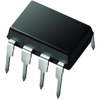
PIC12C672-10/P Microchip Technology, PIC12C672-10/P Datasheet - Page 394

PIC12C672-10/P
Manufacturer Part Number
PIC12C672-10/P
Description
IC,MICROCONTROLLER,8-BIT,PIC CPU,CMOS,DIP,8PIN,PLASTIC
Manufacturer
Microchip Technology
Series
PIC® 12Cr
Datasheets
1.PIC16F688T-ISL.pdf
(688 pages)
2.PIC12CE673-10P.pdf
(129 pages)
3.PIC12CE673-10P.pdf
(14 pages)
Specifications of PIC12C672-10/P
Rohs Compliant
YES
Core Processor
PIC
Core Size
8-Bit
Speed
10MHz
Peripherals
POR, WDT
Number Of I /o
5
Program Memory Size
3.5KB (2K x 14)
Program Memory Type
OTP
Ram Size
128 x 8
Voltage - Supply (vcc/vdd)
3 V ~ 5.5 V
Data Converters
A/D 4x8b
Oscillator Type
Internal
Operating Temperature
0°C ~ 70°C
Package / Case
8-DIP (0.300", 7.62mm)
Processor Series
PIC12C
Core
PIC
Data Bus Width
8 bit
Data Ram Size
128 B
Maximum Clock Frequency
10 MHz
Number Of Programmable I/os
5
Number Of Timers
1
Operating Supply Voltage
3 V to 5.5 V
Maximum Operating Temperature
+ 70 C
Mounting Style
Through Hole
3rd Party Development Tools
52715-96, 52716-328, 52717-734
Development Tools By Supplier
ICE2000
Minimum Operating Temperature
0 C
On-chip Adc
8 bit, 4 Channel
Lead Free Status / RoHS Status
Lead free / RoHS Compliant
For Use With
ISPICR1 - ADAPTER IN-CIRCUIT PROGRAMMINGAC124001 - MODULE SKT PROMATEII 8DIP/SOIC
Eeprom Size
-
Connectivity
-
Lead Free Status / Rohs Status
Details
- Current page: 394 of 688
- Download datasheet (3Mb)
PICmicro MID-RANGE MCU FAMILY
21.7
DS31021A-page 21-10
A/D Conversions
Example 21-2
inputs. The analog reference (V
conversion clock is F
Clearing the GO/DONE bit during a conversion will abort the current conversion. The ADRES
register will NOT be updated with the partially completed A/D conversion sample. That is, the
ADRES register will continue to contain the value of the last completed conversion (or the last
value written to the ADRES register). After the A/D conversion is aborted, a 2T
before the next acquisition is started. After this 2T
on the selected channel.
Example 21-2:
Figure 21-4: A/D Conversion T
;
;
;
;
Note:
Ensure that the required sampling time for the selected input
channel has elapsed. Then the conversion may be started.
BSF
CLRF
BSF
BCF
MOVLW
MOVWF
BCF
BSF
BSF
BSF
Set GO bit
T
:
:
:
AD
1 T
The GO/DONE bit should NOT be set in the same instruction that turns on the A/D,
due to the required acquition time requirement.
Holding capacitor is disconnected
from analog input
show how to perform an A/D conversion. The I/O pins are configured as analog
STATUS, RP0
ADCON1
PIE1,
STATUS, RP0
0xC1
ADCON0
PIR1,
INTCON, PEIE
INTCON, GIE
ADCON0, GO
AD
b7
Doing an A/D Conversion
2 T
RC
. The conversion is performed on the AN0 channel.
AD
b6
ADIE
ADIF
3 T
AD
b5
REF
AD
4 T
) is the device V
Cycles
; Select Bank1
; Configure A/D inputs
; Enable A/D interrupts
; Select Bank0
; RC Clock, A/D is on, Channel 0 is selected
;
; Clear A/D interrupt flag bit
; Enable peripheral interrupts
; Enable all interrupts
; Start A/D Conversion
; The ADIF bit will be set and the GO/DONE
; bit is cleared upon completion of the
;
b4
AD
5 T
A/D Conversion.
Holding capacitor is connected to analog input
b3
AD
6 T
AD
DD
wait, an acquisition is automatically started
. The A/D interrupt is enabled, and the A/D
b2
AD
Next Q4: ADRES is loaded
7 T
AD
b1
8 T
GO bit is cleared
ADIF bit is set
1997 Microchip Technology Inc.
AD
b0
9 T
AD
b0
AD
10
wait is required
T
AD
11
Related parts for PIC12C672-10/P
Image
Part Number
Description
Manufacturer
Datasheet
Request
R

Part Number:
Description:
IC MCU OTP 2KX14 A/D 8DIP
Manufacturer:
Microchip Technology
Datasheet:

Part Number:
Description:
IC MCU OTP 2KX14 A/D 8-SOIJ
Manufacturer:
Microchip Technology
Datasheet:

Part Number:
Description:
IC MCU OTP 2KX14 A/D 8-SOIJ
Manufacturer:
Microchip Technology
Datasheet:

Part Number:
Description:
IC MCU OTP 2KX14 A/D 8-SOIJ
Manufacturer:
Microchip Technology
Datasheet:

Part Number:
Description:
IC MCU OTP 2KX14 A/D 8DIP
Manufacturer:
Microchip Technology
Datasheet:

Part Number:
Description:
IC MCU OTP 2KX14 A/D 8-SOIJ
Manufacturer:
Microchip Technology
Datasheet:

Part Number:
Description:
IC MCU OTP 2KX14 A/D 8DIP
Manufacturer:
Microchip Technology
Datasheet:

Part Number:
Description:
IC MCU OTP 2KX14 A/D 8DFN
Manufacturer:
Microchip Technology
Datasheet:

Part Number:
Description:
IC PIC MCU 2KX14 8DFN
Manufacturer:
Microchip Technology
Datasheet:

Part Number:
Description:
IC MCU OTP 2KX14 A/D 8-SOIJ
Manufacturer:
Microchip Technology
Datasheet:

Part Number:
Description:
IC MCU OTP 2KX14 A/D 8DFN
Manufacturer:
Microchip Technology
Datasheet:

Part Number:
Description:
IC MCU OTP 2KX14 A/D 8DIP
Manufacturer:
Microchip Technology
Datasheet:

Part Number:
Description:
IC MCU OTP 2KX14 A/D 8-SOIJ
Manufacturer:
Microchip Technology
Datasheet:

Part Number:
Description:
IC MCU EPROM 2KX14 A/D 8CDIP
Manufacturer:
Microchip Technology
Datasheet:

Part Number:
Description:
IC,MICROCONTROLLER,8-BIT,PIC CPU,CMOS,DIP,8PIN,PLASTIC
Manufacturer:
Microchip Technology
Datasheet:


