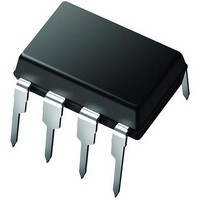
PIC12C672-10/P Microchip Technology, PIC12C672-10/P Datasheet - Page 404

PIC12C672-10/P
Manufacturer Part Number
PIC12C672-10/P
Description
IC,MICROCONTROLLER,8-BIT,PIC CPU,CMOS,DIP,8PIN,PLASTIC
Manufacturer
Microchip Technology
Series
PIC® 12Cr
Datasheets
1.PIC16F688T-ISL.pdf
(688 pages)
2.PIC12CE673-10P.pdf
(129 pages)
3.PIC12CE673-10P.pdf
(14 pages)
Specifications of PIC12C672-10/P
Rohs Compliant
YES
Core Processor
PIC
Core Size
8-Bit
Speed
10MHz
Peripherals
POR, WDT
Number Of I /o
5
Program Memory Size
3.5KB (2K x 14)
Program Memory Type
OTP
Ram Size
128 x 8
Voltage - Supply (vcc/vdd)
3 V ~ 5.5 V
Data Converters
A/D 4x8b
Oscillator Type
Internal
Operating Temperature
0°C ~ 70°C
Package / Case
8-DIP (0.300", 7.62mm)
Processor Series
PIC12C
Core
PIC
Data Bus Width
8 bit
Data Ram Size
128 B
Maximum Clock Frequency
10 MHz
Number Of Programmable I/os
5
Number Of Timers
1
Operating Supply Voltage
3 V to 5.5 V
Maximum Operating Temperature
+ 70 C
Mounting Style
Through Hole
3rd Party Development Tools
52715-96, 52716-328, 52717-734
Development Tools By Supplier
ICE2000
Minimum Operating Temperature
0 C
On-chip Adc
8 bit, 4 Channel
Lead Free Status / RoHS Status
Lead free / RoHS Compliant
For Use With
ISPICR1 - ADAPTER IN-CIRCUIT PROGRAMMINGAC124001 - MODULE SKT PROMATEII 8DIP/SOIC
Eeprom Size
-
Connectivity
-
Lead Free Status / Rohs Status
Details
- Current page: 404 of 688
- Download datasheet (3Mb)
PICmicro MID-RANGE MCU FAMILY
22.1
DS31022A-page 22-2
Introduction
Basic 8-bit
Converter
A/D
This Analog-to-Digital (A/D) converter module has four analog inputs.
The A/D allows conversion of an analog input signal to a corresponding 8-bit digital number. The
output of the sample and hold is the input into the converter, which generates the result via suc-
cessive approximation. The analog reference voltage is software selectable to either the device’s
positive supply voltage (V
unique feature of being able to operate while the device is in SLEEP mode.
The A/D module has three registers. These registers are:
The ADCON0 register, shown in
ADCON1 register, shown in
can be configured as analog inputs (or a voltage reference) or as digital I/O.
Figure 22-1:
• A/D Result Register (ADRES)
• A/D Control Register0 (ADCON0)
• A/D Control Register1 (ADCON1)
(Reference
voltage)
V
REF
Basic 8-bit A/D Block Diagram
(Input voltage)
PCFG1:PCFG0
V
AIN
DD
) or the voltage level on the AN3/V
Figure
V
Figure 22-1
22-2, configures the functions of the port pins. The port pins
DD
00 or
10 or
11
01
controls the operation of the A/D module. The
CHS1:CHS0
11
10
01
00
REF
pin. The A/D converter has a
1997 Microchip Technology Inc.
AN1
AN2
AN0
AN3/V
REF
Related parts for PIC12C672-10/P
Image
Part Number
Description
Manufacturer
Datasheet
Request
R

Part Number:
Description:
IC MCU OTP 2KX14 A/D 8DIP
Manufacturer:
Microchip Technology
Datasheet:

Part Number:
Description:
IC MCU OTP 2KX14 A/D 8-SOIJ
Manufacturer:
Microchip Technology
Datasheet:

Part Number:
Description:
IC MCU OTP 2KX14 A/D 8-SOIJ
Manufacturer:
Microchip Technology
Datasheet:

Part Number:
Description:
IC MCU OTP 2KX14 A/D 8-SOIJ
Manufacturer:
Microchip Technology
Datasheet:

Part Number:
Description:
IC MCU OTP 2KX14 A/D 8DIP
Manufacturer:
Microchip Technology
Datasheet:

Part Number:
Description:
IC MCU OTP 2KX14 A/D 8-SOIJ
Manufacturer:
Microchip Technology
Datasheet:

Part Number:
Description:
IC MCU OTP 2KX14 A/D 8DIP
Manufacturer:
Microchip Technology
Datasheet:

Part Number:
Description:
IC MCU OTP 2KX14 A/D 8DFN
Manufacturer:
Microchip Technology
Datasheet:

Part Number:
Description:
IC PIC MCU 2KX14 8DFN
Manufacturer:
Microchip Technology
Datasheet:

Part Number:
Description:
IC MCU OTP 2KX14 A/D 8-SOIJ
Manufacturer:
Microchip Technology
Datasheet:

Part Number:
Description:
IC MCU OTP 2KX14 A/D 8DFN
Manufacturer:
Microchip Technology
Datasheet:

Part Number:
Description:
IC MCU OTP 2KX14 A/D 8DIP
Manufacturer:
Microchip Technology
Datasheet:

Part Number:
Description:
IC MCU OTP 2KX14 A/D 8-SOIJ
Manufacturer:
Microchip Technology
Datasheet:

Part Number:
Description:
IC MCU EPROM 2KX14 A/D 8CDIP
Manufacturer:
Microchip Technology
Datasheet:

Part Number:
Description:
IC,MICROCONTROLLER,8-BIT,PIC CPU,CMOS,DIP,8PIN,PLASTIC
Manufacturer:
Microchip Technology
Datasheet:


