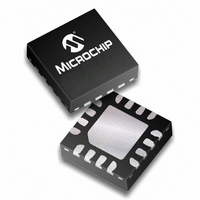
PIC16F676-E/ML Microchip Technology, PIC16F676-E/ML Datasheet - Page 28

PIC16F676-E/ML
Manufacturer Part Number
PIC16F676-E/ML
Description
1.75KB Flash, 64 RAM, 12 I/O 16 QFN 4x4mm TUBE
Manufacturer
Microchip Technology
Series
PIC® 16Fr
Datasheets
1.PIC16F616T-ISL.pdf
(8 pages)
2.PIC12F629T-ISN.pdf
(24 pages)
3.PIC16F630-ISL.pdf
(132 pages)
4.PIC16F630-ISL.pdf
(2 pages)
5.PIC16F630-ISL.pdf
(10 pages)
Specifications of PIC16F676-E/ML
Core Processor
PIC
Core Size
8-Bit
Speed
20MHz
Peripherals
Brown-out Detect/Reset, POR, WDT
Number Of I /o
12
Program Memory Size
1.75KB (1K x 14)
Program Memory Type
FLASH
Eeprom Size
128 x 8
Ram Size
64 x 8
Voltage - Supply (vcc/vdd)
2 V ~ 5.5 V
Data Converters
A/D 8x10b
Oscillator Type
Internal
Operating Temperature
-40°C ~ 125°C
Package / Case
16-QFN
Lead Free Status / RoHS Status
Lead free / RoHS Compliant
For Use With
AC164324 - MODULE SKT FOR MPLAB 8DFN/16QFN
Connectivity
-
Lead Free Status / RoHS Status
Lead free / RoHS Compliant, Lead free / RoHS Compliant
- PIC16F616T-ISL PDF datasheet
- PIC12F629T-ISN PDF datasheet #2
- PIC16F630-ISL PDF datasheet #3
- PIC16F630-ISL PDF datasheet #4
- PIC16F630-ISL PDF datasheet #5
- Current page: 28 of 132
- Download datasheet (2Mb)
PIC16F630/676
3.3
PORTC is a general purpose I/O port consisting of 6
bidirectional pins. The pins can be configured for either
digital I/O or analog input to A/D converter. For specific
information about individual functions such as the
comparator or the A/D, refer to the appropriate section
in this Data Sheet.
EXAMPLE 3-2:
3.3.1
The RC0/RC1/RC2/RC3 pins are configurable to
function as one of the following:
• a general purpose I/O
• an analog input for the A/D Converter
FIGURE 3-6:
DS40039F-page 28
PORTC
PORTC
TRISC
TRISC
BCF
CLRF
BSF
CLRF
MOVLW
MOVWF
BCF
Data bus
WR
WR
Note:
(PIC16F676 only)
RD
RD
PORTC
D
D
STATUS,RP0
PORTC
STATUS,RP0
ANSEL
0Ch
TRISC
STATUS,RP0
To A/D Converter
CK
CK
The ANSEL register (91h) must be clear to
configure an analog channel as a digital
input. Pins configured as analog inputs will
read ‘0’. The ANSEL register is defined for
the PIC16F676.
RC0/AN4, RC1/AN5, RC2/AN6, RC3/
AN7
Q
Q
Q
Q
INITIALIZING PORTC
BLOCK DIAGRAM OF
RC0/RC1/RC2/RC3 PINs
Analog Input
;Bank 0
;Init PORTC
;Bank 1
;digital I/O
;Set RC<3:2> as inputs
;and set RC<5:4,1:0>
;as outputs
;Bank 0
Mode
V
V
DD
SS
I/O Pin
3.3.2
The RC4 and RC5 pins are configurable to function as
a general purpose I/Os.
FIGURE 3-7:
PORTC
PORTC
TRISC
TRISC
Data bus
WR
WR
RD
RD
D
D
CK
CK
RC4 AND RC5
Q
Q
Q
Q
BLOCK DIAGRAM OF RC4
AND RC5 PINS
2010 Microchip Technology Inc.
V
V
DD
SS
I/O Pin
Related parts for PIC16F676-E/ML
Image
Part Number
Description
Manufacturer
Datasheet
Request
R

Part Number:
Description:
IC MCU FLASH 1K W/AD 14-SOIC
Manufacturer:
Microchip Technology
Datasheet:

Part Number:
Description:
IC MCU FLASH 1K W/AD 14-DIP
Manufacturer:
Microchip Technology
Datasheet:

Part Number:
Description:
IC MCU FLASH 1K W/AD 14-TSSOP
Manufacturer:
Microchip Technology
Datasheet:

Part Number:
Description:
IC MCU FLASH 1KX14 W/AD 14DIP
Manufacturer:
Microchip Technology
Datasheet:

Part Number:
Description:
14 PIN, 1.75KB STD FLASH, 64 RAM, 12 I/O,
Manufacturer:
Microchip Technology
Datasheet:

Part Number:
Description:
IC,MICROCONTROLLER,8-BIT,PIC CPU,CMOS,TSSOP,14PIN,PLASTIC
Manufacturer:
Microchip Technology
Datasheet:

Part Number:
Description:
1.75 KB Flash, 64 RAM, 12 I/O 16 QFN 4x4mm TUBE
Manufacturer:
Microchip Technology
Datasheet:

Part Number:
Description:
14-pin, Flash-based 8-bit Cmos Microcontroller
Manufacturer:
Microchip Technology Inc.
Datasheet:

Part Number:
Description:
IC, 8BIT MCU, PIC16F, 32MHZ, SOIC-18
Manufacturer:
Microchip Technology
Datasheet:

Part Number:
Description:
IC, 8BIT MCU, PIC16F, 32MHZ, SSOP-20
Manufacturer:
Microchip Technology
Datasheet:

Part Number:
Description:
IC, 8BIT MCU, PIC16F, 32MHZ, DIP-18
Manufacturer:
Microchip Technology
Datasheet:

Part Number:
Description:
IC, 8BIT MCU, PIC16F, 32MHZ, QFN-28
Manufacturer:
Microchip Technology
Datasheet:

Part Number:
Description:
IC, 8BIT MCU, PIC16F, 32MHZ, QFN-28
Manufacturer:
Microchip Technology
Datasheet:

Part Number:
Description:
IC, 8BIT MCU, PIC16F, 32MHZ, QFN-28
Manufacturer:
Microchip Technology
Datasheet:

Part Number:
Description:
IC, 8BIT MCU, PIC16F, 32MHZ, SSOP-20
Manufacturer:
Microchip Technology
Datasheet:


