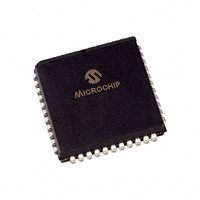
PIC18F448-I/L Microchip Technology, PIC18F448-I/L Datasheet - Page 106

PIC18F448-I/L
Manufacturer Part Number
PIC18F448-I/L
Description
IC,MICROCONTROLLER,8-BIT,PIC CPU,CMOS,LDCC,44PIN,PLASTIC
Manufacturer
Microchip Technology
Series
PIC® 18Fr
Datasheets
1.PIC18LF242-ISO.pdf
(36 pages)
2.PIC18F248-ISO.pdf
(402 pages)
3.PIC18F248-ISO.pdf
(8 pages)
Specifications of PIC18F448-I/L
Rohs Compliant
YES
Core Processor
PIC
Core Size
8-Bit
Speed
40MHz
Connectivity
CAN, I²C, SPI, UART/USART
Peripherals
Brown-out Detect/Reset, LVD, POR, PWM, WDT
Number Of I /o
33
Program Memory Size
16KB (8K x 16)
Program Memory Type
FLASH
Eeprom Size
256 x 8
Ram Size
768 x 8
Voltage - Supply (vcc/vdd)
4.2 V ~ 5.5 V
Data Converters
A/D 8x10b
Oscillator Type
External
Operating Temperature
-40°C ~ 85°C
Package / Case
44-PLCC
Processor Series
PIC18F
Core
PIC
Data Bus Width
8 bit
Data Ram Size
768 B
Interface Type
SPI, I2C, USART
Maximum Clock Frequency
40 MHz
Number Of Programmable I/os
33
Number Of Timers
4
Operating Supply Voltage
2 V to 5.5 V
Maximum Operating Temperature
+ 85 C
Mounting Style
SMD/SMT
3rd Party Development Tools
52715-96, 52716-328, 52717-734, 52712-325, EWPIC18
Development Tools By Supplier
PG164130, DV164035, DV244005, DV164005, PG164120, ICE2000, DV164136, DM163011
Minimum Operating Temperature
- 40 C
On-chip Adc
10 bit, 8 Channel
Lead Free Status / RoHS Status
Contains lead / RoHS non-compliant
For Use With
AC164309 - MODULE SKT FOR PM3 44PLCC444-1001 - DEMO BOARD FOR PICMICRO MCUDVA16XL441 - ADAPTER DEVICE ICE 44PLCCDV007003 - PROGRAMMER UNIVERSAL PROMATE II
Lead Free Status / Rohs Status
Details
Other names
PIC18F448I/L
Available stocks
Company
Part Number
Manufacturer
Quantity
Price
Company:
Part Number:
PIC18F448-I/L
Manufacturer:
Microchip Technology
Quantity:
10 000
- Current page: 106 of 402
- Download datasheet (7Mb)
9.5
PORTE is a 3-bit wide, bidirectional port. PORTE has
three pins (RE0/AN5/RD, RE1/AN6/WR/C1OUT and
RE2/AN7/CS/C2OUT) which are individually config-
urable as inputs or outputs. These pins have Schmitt
Trigger input buffers.
Read-modify-write operations on the LATE register,
read and write the latched output value for PORTE.
The corresponding Data Direction register for the port
is TRISE. Setting a TRISE bit (= 1) will make the
corresponding PORTE pin an input (i.e., put the corre-
sponding output driver in a high-impedance mode).
Clearing a TRISE bit (= 0) will make the corresponding
PORTE pin an output (i.e., put the contents of the
output latch on the selected pin).
The TRISE register also controls the operation of the
Parallel Slave Port through the control bits in the upper
half of the register. These are shown in Register 9-1.
FIGURE 9-10:
DS41159E-page 104
PIC18FXX8
Note:
Note 1: I/O pins have diode protection to V
Peripheral Out Select
Peripheral Data Out
RD LATE
WR TRISE
RD TRISE
Peripheral Enable
RD PORTE
Peripheral Data In
Data Bus
WR LATE
or
WR PORTE
PORTE, TRISE and LATE
Registers
This port is only available on the
PIC18F448 and PIC18F458.
PORTE BLOCK DIAGRAM
TRIS Latch
Data
D
D
CK
CK
Latch
Q
Q
Q
Q
DD
Override
TRIS
and V
0
1
Q
SS
.
EN
D
When the Parallel Slave Port is active, the PORTE pins
function as its control inputs. For additional details,
refer to Section 10.0 “Parallel Slave Port”.
PORTE pins are also multiplexed with inputs for the A/D
converter and outputs for the analog comparators. When
selected as an analog input, these pins will read as ‘0’s.
Direction bits TRISE<2:0> control the direction of the RE
pins, even when they are being used as analog inputs.
The user must make sure to keep the pins configured as
inputs when using them as analog inputs.
EXAMPLE 9-5:
CLRF
CLRF
MOVLW
MOVWF
Schmitt
Trigger
V
V
P
N
SS
DD
PORTE
LATE
03h
TRISE
I/O pin
RE0
RE1
RE2
Pin
INITIALIZING PORTE
; Initialize PORTE by
; clearing output
; data latches
; Alternate method
; to clear output
; data latches
; Value used to
; initialize data
; direction
; Set RE1:RE0 as inputs
; RE2 as an output
; (RE4=0 - PSPMODE Off)
© 2006 Microchip Technology Inc.
(1)
TRIS OVERRIDE
Override Peripheral
Yes
Yes
Yes
PSP
PSP
PSP
Related parts for PIC18F448-I/L
Image
Part Number
Description
Manufacturer
Datasheet
Request
R

Part Number:
Description:
IC, 8BIT MCU, PIC18F, 40MHZ, LCC-44
Manufacturer:
Microchip Technology
Datasheet:

Part Number:
Description:
IC, 8BIT MCU, PIC18LF, 40MHZ, PLCC-64
Manufacturer:
Microchip Technology
Datasheet:

Part Number:
Description:
IC, 8BIT MCU, PIC18F, 64MHZ, TQFP-80
Manufacturer:
Microchip Technology
Datasheet:

Part Number:
Description:
MCU, MPU & DSP Development Tools CAN/LIN PICtail Plus Daughter Board
Manufacturer:
Microchip Technology
Datasheet:

Part Number:
Description:
IC, 8BIT MCU, PIC18F, 64MHZ, DIP-40
Manufacturer:
Microchip Technology
Datasheet:

Part Number:
Description:
IC, 8BIT MCU, PIC18LF, 40MHZ, PLCC-64
Manufacturer:
Microchip Technology
Datasheet:

Part Number:
Description:
IC, 8BIT MCU, PIC18F, 64MHZ, TQFP-64
Manufacturer:
Microchip Technology

Part Number:
Description:
IC, 8BIT MCU, PIC18F, 64MHZ, TQFP-80
Manufacturer:
Microchip Technology

Part Number:
Description:
8KB, Flash, 768bytes-RAM, 36I/O, 8-bit Family,nanowatt XLP 40 UQFN 5x5x0.5mm TUB
Manufacturer:
Microchip Technology
Datasheet:

Part Number:
Description:
8KB, Flash, 768bytes-RAM, 36I/O, 8-bit Family,nanowatt XLP 40 UQFN 5x5x0.5mm TUB
Manufacturer:
Microchip Technology

Part Number:
Description:
16KB, Flash, 768bytes-RAM, 36I/O, 8-bit Family,nanowatt XLP 40 UQFN 5x5x0.5mm TU
Manufacturer:
Microchip Technology
Datasheet:

Part Number:
Description:
16KB, Flash, 768bytes-RAM, 36I/O, 8-bit Family,nanowatt XLP 40 UQFN 5x5x0.5mm TU
Manufacturer:
Microchip Technology

Part Number:
Description:
32KB, Flash, 1536bytes-RAM, 36I/O, 8-bit Family,nanowatt XLP 40 UQFN 5x5x0.5mm T
Manufacturer:
Microchip Technology
Datasheet:

Part Number:
Description:
32KB, Flash, 1536bytes-RAM, 36I/O, 8-bit Family,nanowatt XLP 40 UQFN 5x5x0.5mm T
Manufacturer:
Microchip Technology

Part Number:
Description:
64KB, Flash, 3968bytes-RAM, 36I/O, 8-bit Family,nanowatt XLP 40 UQFN 5x5x0.5mm T
Manufacturer:
Microchip Technology
Datasheet:


