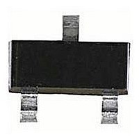
SST201-T1-E3 Vishay, SST201-T1-E3 Datasheet - Page 4

SST201-T1-E3
Manufacturer Part Number
SST201-T1-E3
Description
N CHANNEL JFET, -40V, TO-236
Manufacturer
Vishay
Datasheet
1.SST204-E3.pdf
(6 pages)
Specifications of SST201-T1-E3
Breakdown Voltage Vbr
-40V
Gate-source Cutoff Voltage Vgs(off) Max
-1.5V
Power Dissipation Pd
350mW
Operating Temperature Range
-55°C To +150°C
No. Of Pins
3
Peak Reflow Compatible (260 C)
Yes
Continuous Drain Current Id
200µA
Rohs Compliant
Yes
Transistor Type
JFET
Zero Gate Voltage Drain Current Idss
200µA To 1mA
Lead Free Status / RoHS Status
Lead free / RoHS Compliant
Available stocks
Company
Part Number
Manufacturer
Quantity
Price
Company:
Part Number:
SST201-T1-E3
Manufacturer:
SIEMENS
Quantity:
100
J/SST201 Series
Vishay Siliconix
www.vishay.com
4
TYPICAL CHARACTERISTICS (T
500
400
300
200
100
200
160
120
1.5
1.2
0.9
0.6
0.3
80
40
0
0
0
0
0.01
0
Transconductance vs. Gate-Source Voltage
V
V
GS(off)
GS(off)
Circuit Voltage Gain vs. Drain Current
A
Assume V
R
125_C
V
L
−0.1
−0.1
+
T
+
= −0.7 V
= −0.7 V
A
−1.5 V
V
Transfer Characteristics
T
= −55_C
V
1 ) R
10 V
GS
A
GS
I
125_C
D
= −55_C
DD
g
− Gate-Source Voltage (V)
I
fs
D
− Gate-Source Voltage (V)
= 15 V, V
− Drain Current (mA)
R
−0.2
L
L
−0.2
g
os
0.1
25_C
25_C
DS
−0.3
= 5 V
V
−0.3
GS(off)
V
V
f = 1 kHz
= −0.7 V
DS
DS
= 10 V
−0.4
= 10 V
−0.4
A
= 25_C UNLESS OTHERWISE NOTED)
−0.5
−0.5
1
2000
1600
1200
800
400
3.2
2.4
1.6
0.8
1.6
1.2
0.8
0.4
4
0
0
2
0
0.01
0
0
Transconductance vs. Gate-Source Voltage
V
V
GS(off)
GS(off)
125_C
T
A
125_C
On-Resistance vs. Drain Current
T
V
−0.4
A
= −55_C
−0.4
GS(off)
= −1.5 V
= −55_C
= −1.5 V
V
V
Transfer Characteristics
GS
GS
25_C
= −0.7 V
I
D
− Gate-Source Voltage (V)
− Gate-Source Voltage (V)
25_C
− Drain Current (mA)
−0.8
−0.8
−1.5 V
0.1
S-40393—Rev. G, 15-Mar-04
−1.2
−1.2
Document Number: 70233
V
f = 1 kHz
V
DS
DS
= 10 V
−1.6
= 10 V
−1.6
−2
−2
1


