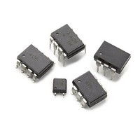
ASSR-4111-301E Avago Technologies US Inc., ASSR-4111-301E Datasheet
ASSR-4111-301E
Specifications of ASSR-4111-301E
Available stocks


Related parts for ASSR-4111-301E


ASSR-4111-301E Summary of contents
Page 1
... Single and Dual Channel Normally-off Single-Pole- Single-Throw (SPST) Relay • 400V Output Withstand Voltage • 0.12A or 0.24A Current Rating (See Schematic for ASSR-4111 Connection A and B) • Low Input Current: CMOS Compatibility • Low On-Resistance: 5.5Ω Typical for DC-only, 16Ω Typical for AC/DC • ...
Page 2
... Ordering Information ASSR-xxxx is UL Recognized with 3750 Vrms for 1 minute per UL1577 and is approved under CSA Component Ac- ceptance Notice #5, File CA 88324. Option Part number RoHS Compliant -003E ASSR-4110 -503E -001E ASSR-4111 -301E -501E -002E ASSR-4120 -302E -502E ASSR-4130 -005E (Preliminary Product ...
Page 3
... ASSR-4111 Connection A Opto -isolation Opto -isolation ASSR-4111 Connection B Opto -isolation ASSR-4120 and ASSR-4130 Opto-isolation Opto -isolation Opto -isolation 1 1 Equivalent Equivalent Relay Relay Vo Vo Diagram Diagram 2 2 Opto -isolation Equivalent 5 Relay - Diagram 2 Opto-isolation 1 2 Equivalent Relay Diagram and ...
Page 4
... Package Outline Drawings ASSR-4110 4-Pin Small Outline Package 2.54 (0.100) LEAD FREE xxxx 4.40±0.20 YWW (0.173±0.008) (0.268±0.016) 0.375 0.41 (0.015) (0.016) 4.3±0.2 (0.169±0.008) DIMENSIONS IN MILLIMETERS AND (INCHES) OPTION NUMBER 500 AND UL RECOGNITION NOT MARKED ASSR-4111 6-Pin DIP Package 9 ...
Page 5
... ASSR-4111 6-Pin DIP Package with Gull Wing Surface Mount Option 300 9.65 ± 0.25 (0.380 ± 0.010) 6.35 ± 0.25 (0.250 ± 0.010) 1.78 (0.070) MAX. 4.19 MAX. (0.165) 2.54 (0.100) 2.29 TYP. (0.090) NOTE: FLOATING LEAD PROTRUSION IS 0.25 mm (10 mils) MAX. ...
Page 6
... ASSR-4120 8-Pin DIP Package with Gull Wing Surface Mount Option 300 9.65 ± 0.25 (0.380 ± 0.010 1.19 (0.047) MAX. 1.080 ± 0.320 (0.043 ± 0.013) 2.54 (0.100) BSC DIMENSIONS IN MILLIMETERS (INCHES). LEAD COPLANARITY = 0.10 mm (0.004 INCHES). NOTE: FLOATING LEAD PROTRUSION IS 0.25 mm (10 mils) MAX. ...
Page 7
... C T smax smin Non-halide flux should be used. Regulatory Information The ASSR-4110, ASSR-4111, ASSR-4120 and ASSR-4130 (Preliminary Product Release) are approved by the following organizations: UL Approvals under UL 1577, component recognition program Approvals under CSA Component Acceptance Notice #5. Insulation and Safety Related Specifications ...
Page 8
... ASSR-4120 and ASSR-4130 Output Power Dissipation ASSR-4110 ASSR-4111 ASSR-4120 and ASSR-4130 Average Output Current ≤ 25°C, T 100° ASSR-4111 Con- nection B Output Voltage (T = 25°C) A ASSR-4111 Con- nection B Solder Reflow Temperature Profile Recommended Operating Conditions Parameter Symbol Input Current (ON) I F(ON) ...
Page 9
... Voltage Output Leakage I O(OFF) Current Output Offset |V | (OS) Voltage Input Reverse V R Breakdown Voltage Input Forward V F Voltage Output R (ON) On-resistance ASSR-4111 Con- nection B 9 Min. Typ. Max. Units 3750 Vrms Ω 0.4 pF 0.5 pF 0 5mA to 10mA, unless otherwise specified. F Min ...
Page 10
... ASSR-4110 - pin 1, 2 shorted and pin 3, 4 shorted. ASSR-4111 - pin shorted and pin shorted. ASSR-4120 and ASSR-4130 - pin shorted and pin shorted. 5. The Input-Output Momentary Withstand Voltage is a dielectric voltage rating that should not be interpreted as an input-output continuous voltage rating. For the continuous voltage rating refer to the IEC/EN/DIN EN 60747-5-2 Insulation Characteristics Table (if applicable), your equipment level safety specification, or Avago Technologies Application Note 1074, “ ...
Page 11
... MOSFET junction temperature remains less than 125°C. Turn On Time and Turn Off Time Variation The ASSR-41xx Series exhibits a very fast turn on and turn off time. Both the turn on and turn off time can be adjusted by choosing proper forward current as depicted in Figures 11 and 13. The changes of the turn on and turn off time with ambient temperature are also shown in Figures 12 and 14 ...
Page 12
I =250µ =0.8V F 1.05 1 0.95 0.9 -50 - TEMPERATURE - A Figure 5. Normalized Typical Output Withstand Voltage vs. Temperature 1.5 1.4 I =10mA F 1.3 1.2 I =5mA F 1.1 ...
Page 13
I - INPUT CURRENT - mA F(ON) Figure 11. Typical Turn On Time vs. Input Current ...
Page 14
... PULSE GEN Ω 5ns ASSR-4120 INPUT MONITORING 2 NODE R 200ohm 3 4 INPUT 50 OUTPUT Vo 10 Figure 16. Switching Test circuit for OFF INCLUDES PROBE AND STRAY WIRING 6 5 50% P. 90% t OUTPUT Vo MONITORING NODE IS APPROXIMATELY 25pF WHICH L CAPACITANCE) OFF ...
Page 15
... ASSR-4120 1 INPUT OPEN 90% V PEAK 10 (MAX) < (0.8 OVERSHOOT ON V Figure 17. Output Transient Rejection Test Circuit PEAK 7 + PULSE GEN Ω INCLUDES PROBE AND FIXTURE CAPACITANCE M R INCLUDES PROBE AND FIXTURE RESISTANCE M 90 (0.8)V PEAK PEAK < 10% _ PEAK OUTPUT Vo MONITORING NODE 10% ...
Page 16
... For product information and a complete list of distributors, please go to our web site: Avago, Avago Technologies, and the A logo are trademarks of Avago Technologies in the United States and other countries. Data subject to change. Copyright © 2005-2008 Avago Technologies. All rights reserved. Obsoletes AV02-0279EN - September 16, 2008 V DD ASSR-4120 ...