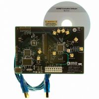
AD9957/PCBZ Analog Devices Inc, AD9957/PCBZ Datasheet - Page 48
AD9957/PCBZ
Manufacturer Part Number
AD9957/PCBZ
Description
D/A Converter Evaluation Board
Manufacturer
Analog Devices Inc
Series
AgileRF™r
Datasheet
1.AD9957BSVZ-REEL.pdf
(64 pages)
Specifications of AD9957/PCBZ
Silicon Manufacturer
Analog Devices
Application Sub Type
Direct Digital Synthesizer
Kit Application Type
Clock & Timing
Silicon Core Number
AD9957
Kit Contents
Board
Main Purpose
Timing: DDS Modulators
Embedded
No
Utilized Ic / Part
AD9957
Primary Attributes
14-Bit DAC, 32-Bit Tuning Word Width
Secondary Attributes
1GHz, Graphical User Interface
Lead Free Status / RoHS Status
Lead free / RoHS Compliant
Available stocks
Company
Part Number
Manufacturer
Quantity
Price
Company:

Part Number:
AD9957/PCBZ
Manufacturer:
LT
Quantity:
962


AD9957
SDO—Serial Data Out
Data is read from this pin for protocols that use separate lines
for transmitting and receiving data. In the case where the
AD9957 operates in a single bidirectional I/O mode, this pin
does not output data and is set to a high impedance state.
I/O_RESET—Input/Output Reset
I/O_RESET synchronizes the I/O port state machines without
affecting the addressable registers contents. An active high
input on the I/O_RESET pin causes the current communication
cycle to abort. After I/O_RESET returns low (Logic 0), another
communication cycle can begin, starting with the instruction
byte write.
I/O_UPDATE—Input/Output Update
The I/O_UPDATE initiates the transfer of written data from
the I/O port buffer to active registers. I/O_UPDATE is active
on the rising edge and its pulse width must be greater than one
SYNC_CLK period. It is either an input or output pin depending
on the programming of the Internal I/O Update Active bit.
SCLK
SDIO
SCLK
SCLK
SDO
SDIO
SCLK
SDIO
SDIO
CS
CS
CS
CS
I
I
7
7
I
I
7
7
I
I
6
6
I
I
6
6
I
INSTRUCTION CYCLE
5
I
INSTRUCTION CYCLE
INSTRUCTION CYCLE
INSTRUCTION CYCLE
5
I
I
5
5
Figure 63. 2-Wire Serial Port Read Timing—Clock Stall High
Figure 61. 3-Wire Serial Port Read Timing—Clock Stall Low
I
I
4
4
Figure 62. Serial Port Write Timing—Clock Stall High
Figure 60. Serial Port Write Timing—Clock Stall Low
I
I
4
4
I
I
3
3
I
I
3
3
I
I
2
2
I
I
2
2
I
Rev. B | Page 48 of 64
I
1
1
I
I
1
1
I
I
0
0
I
0
I
0
D
D
O7
D
7
SERIAL I/O TIMING DIAGRAMS
Figure 60 through Figure 63 provide basic examples of the tim-
ing relationships between the various control signals of the serial
I/O port. Most of the bits in the register map are not transferred
to their internal destinations until assertion of an I/O update,
which is not included in the timing diagrams that follow.
MSB/LSB TRANSFERS
The AD9957 serial port can support both most significant bit
(MSB) first or least significant bit (LSB) first data formats. This
functionality is controlled by Bit 0 in Control Function Register 1
(0x00). The default format is MSB first. If LSB first is active,
all data, including the instruction byte, must follow LSB-first
convention. Note that the highest number found in the bit range
column for each register is the MSB and the lowest number is
the LSB for that register (see the Register Map and Bit
Descriptions section and Table 13).
7
D
O7
D
D
6
O6
D
D
DATA TRANSFER CYCLE
O6
6
DATA TRANSFER CYCLE
D
D
DATA TRANSFER CYCLE
5
DATA TRANSFER CYCLE
O5
D
D
O5
5
D
D
DON'T CARE
4
O4
D
D
4
O4
D
D
3
O3
D
D
3
O3
D
D
2
O2
D
D
2
O2
D
D
1
O1
D
D
1
O1
D
0
D
D
O0
O0
D
0
Related parts for AD9957/PCBZ
Image
Part Number
Description
Manufacturer
Datasheet
Request
R


Part Number:
Description:
±1.7g Dual-Axis IMEMS Accelerometer Evaluation Board
Manufacturer:
Analog Devices Inc
Datasheet:

Part Number:
Description:
Inertial Sensor Evaluation System
Manufacturer:
Analog Devices Inc
Datasheet:
Part Number:
Description:
Manufacturer:
Analog Devices Inc
Datasheet:
Part Number:
Description:
Manufacturer:
Analog Devices Inc
Datasheet:
Part Number:
Description:
Manufacturer:
Analog Devices Inc
Datasheet:
Part Number:
Description:
Manufacturer:
Analog Devices Inc
Datasheet:
Part Number:
Description:
Manufacturer:
Analog Devices Inc
Datasheet:
Part Number:
Description:
Manufacturer:
Analog Devices Inc
Datasheet:
Part Number:
Description:
Manufacturer:
Analog Devices Inc
Datasheet:
Part Number:
Description:
Manufacturer:
Analog Devices Inc
Datasheet:
Part Number:
Description:
Manufacturer:
Analog Devices Inc
Datasheet:
Part Number:
Description:
Manufacturer:
Analog Devices Inc
Datasheet: