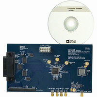
AD9858/PCBZ Analog Devices Inc, AD9858/PCBZ Datasheet - Page 20

AD9858/PCBZ
Manufacturer Part Number
AD9858/PCBZ
Description
DIGITAL SYNTHESIZER
Manufacturer
Analog Devices Inc
Specifications of AD9858/PCBZ
Silicon Manufacturer
Analog Devices
Application Sub Type
Direct Digital Synthesizer
Kit Application Type
Clock & Timing
Silicon Core Number
AD9858
Kit Contents
Board
Design Resources
Low Jitter Sampling Clock Generator for High Performance ADCs Using AD9958/9858 and AD9515 (CN0109)
Main Purpose
Timing, Direct Digital Synthesis (DDS)
Utilized Ic / Part
AD9858/TL
Lead Free Status / RoHS Status
Lead free / RoHS Compliant
Embedded
-
Primary Attributes
-
Secondary Attributes
-
Lead Free Status / RoHS Status
Lead free / RoHS Compliant, Lead free / RoHS Compliant
Other names
AD9858/PCB
AD9858/PCB
AD9858/PCB
AD9858
I/O Port Functionality
The I/O port can operate in either serial or parallel programming
mode. Mode selection is accomplished via the SPSELECT pin.
The ability to read back the contents of a register is provided in
both modes to facilitate the debug process during the user’s
prototyping phase of a design. In either mode, however, the
reading back of profile registers requires that the profile select
pins (PS0 and PS1) be configured to select the desired register
bank. When reading a register that resides in one of the profiles,
the register address acts as an offset to select one of the registers
among the group of registers defined by the profile. The profile
select pins control the base address of the register bank and
select the appropriate register grouping.
ADDR[5:0]
D[7:0]
WR
A
1
SPECIFICATION
t
t
t
t
t
t
t
ASU
DSU
AHU
DHU
WRLOW
WRHIGH
WR
D
1
t
WRHIGH
t
VALUE
3ns
3.5ns
0ns
0ns
3ns
6ns
9ns
ASU
Figure 35. I/O Port Write Cycle Timing (Parallel)
t
WR
DESCRIPTION
ADDRESS SETUP TIME TO WR SIGNAL ACTIVE
DATA SETUP TIME TO WR SIGNAL INACTIVE
ADDRESS HOLD TIME TO WR SIGNAL INACTIVE
DATA HOLD TIME TO WR SIGNAL INACTIVE
WR SIGNAL MINIMUM LOW TIME
WR SIGNAL MINIMUM HIGH TIME
WR SIGNAL MINIMUM PERIOD
t
WRLOW
Rev. C | Page 20 of 32
A
t
2
DSU
D
2
Parallel Programming Mode
In parallel programming mode, the I/O port makes use of eight
bidirectional data pins (D7 to D0), six address input pins (ADDR5
to ADDR0), a read input pin ( RD ), and a write input pin ( WR ).
A register is selected by providing the proper address combination
as defined in the register map (see
functionality is invoked by pulsing the appropriate pin (
WR ); the two operations are mutually exclusive. The read or write
data is transported on the D7 to D0 pins. The correlation between
the D7 to D0 data bits and their functionality at a specific register
address is detailed in the register map (see
bit description.
Parallel I/O operation allows write access to each byte of any
register in the I/O buffer memory in a single I/O operation.
Readback capability is slower than write capability. It is intended as
a low speed function for debug purposes. Timing for both write
and read cycles is depicted in Figure 35 and Figure 36.
t
t
AHU
DHU
A
3
Table 6
). Read or write
Table 6
D
3
) and register
RD or


