CMD-711EX AXIOM, CMD-711EX Datasheet - Page 8
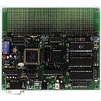
CMD-711EX
Manufacturer Part Number
CMD-711EX
Description
Microprocessor Development Tool
Manufacturer
AXIOM
Datasheet
1.CMD-711EX.pdf
(15 pages)
Specifications of CMD-711EX
Silicon Manufacturer
Freescale
Kit Contents
Board
Silicon Family Name
68HC11E
Silicon Core Number
MC68HC11E9FN, MC68HC11E20FN
Development Tool Type
Hardware - Eval/Demo Board
Lead Free Status / RoHS Status
Contains lead / RoHS non-compliant


ADDRESS DECODING
IC sockets
accommodate EEPROM or ROM but is primarily used for program storage using an EEPROM. Jumpers JP1
through JP7 and Mode Switches 4-5 determine how U5, U6, and U7 are used.
Address decoding is accomplished on the board using a GAL22V10 (U7) programmable logic device. Address lines
A<8:15>, AS (address strobe), R/W (read/write), and E (clock) are processed to provide the memory control signals
as shown below by default. Custom configurations, differing from that shown below, are also possible. Contact the
factory for assistance in redefining the memory map if required.
All of these signals are active low. Signal line M2 is also connected to the BUS_PORT expansion connector allowing
M2 to work in conjunction with the CS and Address lines to implement off board, page banked memory. When M2 is
used in this manner, U6 must be removed from the board.
Peripheral Access 'P' is used in conjunction with A<4:6>, and AS to generate CS<0:7>.
selects controls sixteen bytes in the memory map from B580 through B5FF. CS<7:0> are brought out to the
BUS_PORT where they can be used to control peripherals external to the development board. See the Memory Map
for further clarification. CS7 is used for the LCD_PORT.
Single Chip Mode
To operate the HC11 in "True Single Chip" mode, Mode Switch position 1 should be ON and the BUS_EN jumper
installed to disable bus operation. In this mode BUS_PORT D0-7 are HC11 port C and A8-15 are HC11 port B. In
expanded mode the HC24 Port Replacement Unit (U2) replaces these ports on the MCU_PORT connector.
OE
WE
M1
M2
M3
P
7FFF
0000
U3
and
Output enable to U3, U4, U5 and BUS_PORT
Write enable to U3 direct and to U4 and U5 through jumper JP4 and Mode Switch 3
respectively.
Chip select to U3 active from 0 to 32k, 0000 - 7FFF.
Chip select to U4 active for the 24k between 8000 and DFFF, with the exception of B580
through B7FF inclusive. B580 to B5FF is used by both P and CS0-7. B600 to B7FF is taken
by the HC11 internal EEPROM, if enabled.
Chip select to U7 active for the 8k between D000 and FFFF.
NOTE: Mode switches 4-5 effect the memory map for M2 and M3.
Peripheral Access CS0 - CS7. B580 through B5FF.
U3
U4
hold 32k RAM chips for external data storage and for debugging programs.
CFFF
8000
U4
8
FFFF
D000
U5
Each of these eight chip
U5
can
Related parts for CMD-711EX
Image
Part Number
Description
Manufacturer
Datasheet
Request
R

Part Number:
Description:
Single Board Computer
Manufacturer:
AXIOM
Datasheet:


Part Number:
Description:
General Power Transformer <SMD Type: CMD Series>
Manufacturer:
Sumida Corporation
Part Number:
Description:
Power Inductors <SMD Type: CMD Series>
Manufacturer:
Sumida Corporation
Part Number:
Description:
General Power Transformer <SMD Type: CMD Series>
Manufacturer:
Sumida Corporation

Part Number:
Description:
Linear Regulators - Standard VDDQ/VTT Regulator P2 Fused
Manufacturer:
CMD / ON Semiconductor
Part Number:
Description:
Switching Converters, Regulators & Controllers Charge Pump LDO
Manufacturer:
CMD / ON Semiconductor