CDB42L55 Cirrus Logic Inc, CDB42L55 Datasheet - Page 18
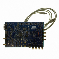
CDB42L55
Manufacturer Part Number
CDB42L55
Description
Eval Bd Ultra Low Power Stereo Codec
Manufacturer
Cirrus Logic Inc
Specifications of CDB42L55
Main Purpose
Audio, CODEC
Embedded
Yes, FPGA / CPLD
Utilized Ic / Part
CS42L55
Primary Attributes
2 Stereo Analog Inputs, Stereo Line and Headphone Outputs, S/PDIF Transmitter and Receiver
Secondary Attributes
GUI, USB, RS232, I2C Interfaces, USB or External or Battery Power Supply
Product
Audio Modules
Lead Free Status / RoHS Status
Contains lead / RoHS non-compliant
Lead Free Status / RoHS Status
Contains lead / RoHS non-compliant
Other names
598-1506
CDB-42L55
CDB-42L55


18
JMP
J31
J36
J25
J28
J52
J74
J53
J48
J22
J12
J34
J11
J7
J5
J4
J2
J3
1.8V Buck Input
HPOUTA(LPF)
HPOUTB(LPF)
Shunt to RCA
Shunt to RCA
Board Power
HP Detect
LABEL
HPOUTB
HPOUTB
HPOUTA
HPOUTA
VLDO
VLDO
VCP
VCP
VL
VA
VA
VL
Selects how the HP_Detect pin on
Provides RCA reference to GND
Provides RCA reference to GND
Selects source of voltage for the
Selects source of voltage for the
Selects source of voltage for the
Selects source of voltage for the
Selects power supply source for
Selects test load from HPOUTA
Selects test load from HPOUTB
Selects source of Board Power
Connects or removes LPF for
Connects or removes LPF for
Current Measurement
CS42L55is driven
PURPOSE
VLDO supply
VCP supply
VL supply
VA supply
HPOUTB
HPOUTA
+1.8VB
Table 2. Jumper Settings
POSITION
*SHUNTED
*SHUNTED
*SHUNTED
+1.8VB
+1.8VB
+1.8VB
+1.8VB
*+1.8V
*+1.8V
*+1.8V
*+1.8V
OPEN
+2.5V
+3.3V
+2.5V
+2.5V
+2.5V
*2 - 3
*2 - 3
*2 - 3
*2 - 3
*2 - 3
1 - 2
1 - 2
1 - 2
2 - 3
1 - 2
2 - 3
1 - 2
1 - 2
1 - 2
Voltage source is +1.8 V regulator.
Voltage source is +2.5 V regulator.
Voltage source is +3.3 V regulator.
Voltage source is +1.8V from battery.
Voltage source is +1.8 V regulator.
Voltage source is +2.5 V regulator. .
Voltage source is +1.8V from battery.
Voltage source is +1.8 V regulator.
Voltage source is +2.5 V regulator. .
Voltage source is +1.8V from battery.
Voltage source is +1.8 V regulator.
Voltage source is +2.5 V regulator. .
Voltage source is +1.8V from battery.
1 Ω series resistor is shorted.
1 Ω series resistor in power supply path.
AIN2B and AIN2A RCAs are given a ground ref-
erence.
AIN1B and AIN1A RCAs are given a ground ref-
erence.
HPDETECT is driven by FPGA/GUI.
HPDETECT is driven by HP Jack line when a
stereo connection is inserted in J1.
1.8VB is derived from external input.
1.8VB is derived from AAA batteries.
32 Ω load selected for HPOUTA.
16 Ω load selected for HPOUTA.
32 Ω load selected for HPOUTB.
16 Ω load selected for HPOUTB.
No filtered output selected for HPOUTA.
RC filtered output selected for HPOUTA.
No filtered output selected for HPOUTB.
RC filtered output selected for HPOUTB.
Board powered from external +5V source con-
nected to TP9/TP10.
Board powered from USB.
FUNCTION SELECTED
*Default factory settings
CDB42L55
DS773DB1
Related parts for CDB42L55
Image
Part Number
Description
Manufacturer
Datasheet
Request
R

Part Number:
Description:
Development Kit
Manufacturer:
Cirrus Logic Inc
Datasheet:
Part Number:
Description:
Development Kit
Manufacturer:
Cirrus Logic Inc
Datasheet:


Part Number:
Description:
High-efficiency PFC + Fluorescent Lamp Driver Reference Design
Manufacturer:
Cirrus Logic Inc
Datasheet:
Part Number:
Description:
Development Kit
Manufacturer:
Cirrus Logic Inc
Datasheet:
Part Number:
Description:
Development Kit
Manufacturer:
Cirrus Logic Inc
Datasheet:

Part Number:
Description:
Development Kit
Manufacturer:
Cirrus Logic Inc
Datasheet:
Part Number:
Description:
Development Kit
Manufacturer:
Cirrus Logic Inc
Datasheet:
Part Number:
Description:
Development Kit
Manufacturer:
Cirrus Logic Inc
Datasheet:
Part Number:
Description:
Development Kit
Manufacturer:
Cirrus Logic Inc
Datasheet:

Part Number:
Description:
EVALUATION BOARD FOR CS8427
Manufacturer:
Cirrus Logic Inc
Datasheet:

Part Number:
Description:
BOARD EVAL FOR CS8416 RCVR
Manufacturer:
Cirrus Logic Inc
Datasheet:

Part Number:
Description:
EVALUATION BOARD FOR CS8420
Manufacturer:
Cirrus Logic Inc
Datasheet:

Part Number:
Description:
KIT DEVELOPMENT EP9315 ARM9
Manufacturer:
Cirrus Logic Inc
Datasheet:

Part Number:
Description:
KIT DEVELOPMENT EP9302 ARM9
Manufacturer:
Cirrus Logic Inc
Datasheet: