HFBR-5963AL Avago Technologies US Inc., HFBR-5963AL Datasheet - Page 2
HFBR-5963AL
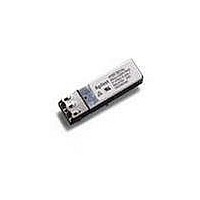
Manufacturer Part Number
HFBR-5963AL
Description
Fiber Optic Transmitters, Receivers, Transceivers OC3/FE 2X5 LC SD LVT TL EXTD TEMP
Manufacturer
Avago Technologies US Inc.
Datasheet
1.HFBR-5963AL.pdf
(13 pages)
Specifications of HFBR-5963AL
Function
Transceivers for ATM, FDDI, Fast Ethernet and SONET OC-3/SDH STM-1 with LC connector.
Product
Transceiver
Data Rate
125 Mbps, 155 Mbps
Wavelength
1300 nm
Maximum Rise Time
3 ns, 2.2 ns
Maximum Fall Time
3 ns, 2.2 ns
Pulse Width Distortion
0.4 ns, 0.3 ns
Maximum Output Current
50 mA
Operating Supply Voltage
2.97 V to 3.63 V
Maximum Operating Temperature
+ 85 C
Minimum Operating Temperature
- 40 C
Package / Case
DIP-10 with Connector
Optical Fiber Type
TX/RX
Data Transfer Rate
155.52MBd
Optical Rise Time
3/2.2ns
Optical Fall Time
3/2.2ns
Jitter
0.4/0.3ns
Operating Temperature Classification
Industrial
Peak Wavelength
1308/1380nm
Package Type
DIP With Connector
Operating Supply Voltage (min)
2.97V
Operating Supply Voltage (typ)
3.3V
Operating Supply Voltage (max)
3.63V
Output Current
50mA
Operating Temp Range
-40C to 85C
Mounting
Snap Fit To Panel
Pin Count
10
For Use With
Multimode Glass
Lead Free Status / RoHS Status
Lead free / RoHS Compliant
Available stocks
Company
Part Number
Manufacturer
Quantity
Price
Company:

Part Number:
HFBR-5963ALZ
Manufacturer:
AVAGO
Quantity:
3 200
Company:
Part Number:
HFBR-5963ALZ
Manufacturer:
Avago Technologies
Quantity:
135
Part Number:
HFBR-5963ALZ
Manufacturer:
AVAGO/安华高
Quantity:
20 000


Transmitter Section
The transmitter section of the HFBR-5963L utilizes a 1300
nm InGaAsP LED. This LED is packaged in the optical sub-
assembly portion of the transmitter section. It is driven
by a custom silicon IC which converts differential PECL
logic signals, ECL referenced (shifted) to a +3.3 V supply,
into an analog LED drive current.
Receiver Section
The receiver section of the HFBR-5963L utilizes an InGaAs
PIN photodiode coupled to a custom silicon transimped-
ance preamplifier IC. It is packaged in the optical subas-
sembly portion of the receiver.
This PIN/preamplifier combination is coupled to a custom
quantizer IC which provides the final pulse shaping for
the logic output and the signal detect function. The data
output is differential. The data output is PECL compat-
ible, ECL referenced (shifted) to a +3.3 V power supply.
The receiver outputs, data output and data out bar, are
squelched at signal detect deassert. The signal detect
output is single ended. The signal detect circuit works by
sensing the level of the received signal and comparing
this level to a reference. The SD output is +3.3 V TTL.
Package
The overall package concept for the Avago Technologies
transceiver consists of three basic elements; the two op-
tical subassemblies, an electrical subassembly, and the
housing as illustrated in the block diagram in Figure 1.
The package outline drawing and pin out are shown in
Figure 1. Block Diagram
DATA IN
DATA IN
DATA OUT
DATA OUT
SIGNAL
DETECT
QUANTIZER IC
LED DRIVER IC
R
T
X
X
SUPPLY
SUPPLY
R
T
X
X
GROUND
GROUND
Figures 2 and 5. The details of this package outline and
pin out are compliant with the multisource definition of
the 2 x 5 DIP. The low profile of the Avago Technologies
transceiver design complies with the maximum height
allowed for the LC connector over the entire length of
the package.
The optical subassemblies utilize a high-volume assem-
bly process together with low-cost lens elements which
result in a cost- effective building block.
The electrical subassembly consists of a high volume mul-
tilayer printed circuit board on which the ICs and various
surface-mounted passive circuit elements are attached.
The receiver section includes an internal shield for the
electrical and optical subassemblies to ensure high im-
munity to external EMI fields.
The outer housing including the LC ports is molded
of filled nonconductive plastic to provide mechanical
strength. The solder posts of the Avago Technologies
design are isolated from the internal circuit of the trans-
ceiver.
The transceiver is attached to a printed circuit board with
the ten signal pins and the two solder posts which exit
the bottom of the housing. The two solder posts provide
the primary mechanical strength to withstand the loads
imposed on the transceiver by mating with the LC con-
nector fiber cables.
PIN PHOTODIODE
PRE-AMPLIFIER
SUBASSEMBLY
LED
OPTICAL
SUBASSEMBLY
LC
RECEPTACLE
Related parts for HFBR-5963AL
Image
Part Number
Description
Manufacturer
Datasheet
Request
R

Part Number:
Description:
RECEIVER FIBER OPTIC 600NM 40KBD
Manufacturer:
Avago Technologies US Inc.
Datasheet:

Part Number:
Description:
XMITTER FIBER OPTIC 600NM 5MBD
Manufacturer:
Avago Technologies US Inc.
Datasheet:

Part Number:
Description:
XMITTER FIBER OPTIC 600NM 40KBD
Manufacturer:
Avago Technologies US Inc.
Datasheet:

Part Number:
Description:
XMITTER VERSATILE LINK HORZ
Manufacturer:
Avago Technologies US Inc.
Datasheet:

Part Number:
Description:
XMITTER OPT HI PERFORMANCE VERT
Manufacturer:
Avago Technologies US Inc.
Datasheet:

Part Number:
Description:
TXRX FIBER OPTIC 650NM 10MBAUD
Manufacturer:
Avago Technologies US Inc.
Datasheet:
Part Number:
Description:
TXRX FIBER OPTIC 650NM 10MBAUD
Manufacturer:
Avago Technologies US Inc.
Datasheet:

Part Number:
Description:
FIBER OPTIC TRANSMITTER 660NM
Manufacturer:
Avago Technologies US Inc.
Datasheet:

Part Number:
Description:
KIT EVAL FIBER OPTIC 5MBD
Manufacturer:
Avago Technologies US Inc.
Datasheet:
Part Number:
Description:
KIT EVAL FIBER OPTICS 32MBD
Manufacturer:
Avago Technologies US Inc.
Datasheet:

Part Number:
Description:
KIT EVAL FIBER OPTIC 5MBD
Manufacturer:
Avago Technologies US Inc.
Datasheet:

Part Number:
Description:
125MBd 1300nm FiberOptic Eval Kit
Manufacturer:
Avago Technologies US Inc.
Datasheet:

Part Number:
Description:
DC-5MBd 820nm FiberOptic EvalKit
Manufacturer:
Avago Technologies US Inc.
Datasheet:
Part Number:
Description:
125MBd 820nm FiberOptic Eval Kit
Manufacturer:
Avago Technologies US Inc.
Datasheet:
Part Number:
Description:
DC-5MBd 650nm POF Eval Kit
Manufacturer:
Avago Technologies US Inc.
Datasheet: