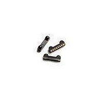
ASDL-3023-021 Avago Technologies US Inc., ASDL-3023-021 Datasheet - Page 18

ASDL-3023-021
Manufacturer Part Number
ASDL-3023-021
Description
Infrared Transceivers SFF FIR+RC Front w/o Shield
Manufacturer
Avago Technologies US Inc.
Datasheet
1.ASDL-3023-021.pdf
(25 pages)
Specifications of ASDL-3023-021
Wavelength
885 nm, 875 nm
Continual Data Transmission
4 Mbit/s
Transmission Distance
30 cm
Radiant Intensity
50 mW/sr
Half Intensity Angle Degrees
15 deg
Pulse Width
4 us, 1.6 us
Maximum Rise Time
60 ns, 600 ns
Maximum Fall Time
60 ns, 600 ns
Led Supply Voltage
- 0.3 V to 6 V
Operating Voltage
2.4 V to 3.6 V
Maximum Operating Temperature
+ 85 C
Minimum Operating Temperature
- 25 C
Dimensions
7.5 mm x 2.75 mm x 1.75 mm
Lead Free Status / RoHS Status
Lead free / RoHS Compliant
Appendix B: PCB Layout Suggestion
The effects of EMI and power supply noise can potentially
reduce the sensitivity of the receiver, resulting in reduced
link distance. The PCB layout played an important role to
obtain a good PSRR and EM immunity resulting in good
electrical performance. Things to note:
1. The ground plane should be continuous under the
2. The shield trace is a wide, low inductance trace back
3. VLED can be connected to either unfiltered or
4. VCC pin can be connected to either unfiltered or
5. IOVCC is connected to the ASIC voltage supply or
8
Layer 3
part, but should not extend under the shield trace.
to the system ground. CX1, CX2, CX3, CX4 and CX5 are
optional supply filter capacitors; they may be left out if
a clean power supply is used.
unregulated power supply. The bypass capacitors
should be connection before the current limiting
resistor R2 respectively. In a noisy environment,
including capacitor CX3and CX4 can enhance supply
rejection. CX3 that is generally a ceramic capacitor of
low inductance providing a wide frequency response
while CX4 is tantalum capacitor of big volume and fast
frequency response. The use of a tantalum capacitor
is more critical on the VLED line, which carries a high
current.
unregulated power supply. The Resistor, R1 together
with the capacitors, CX 1and CX2 acts as the low pass
filter.
the VCC supply. The capacitor, CX5 acts as the bypass
capacitor.
Bottom Layer (GND)
Noise sources to be placed as far away from the transceiver as possible
R
1
CX1
CX2
CX5
R
2
Legend: ground via
CX3
CX4
Layer 2
Top Layer
6. Preferably a multi-layered board should be used
The area underneath the module at the second layer, and
3cm in all direction around the module is defined as the
critical ground plane zone. The ground plane should be
maximized in this zone. Refer to application note AN1114
or the Avago Technologies IrDA Data Link Design Guide
for details. The layout below is based on a 2-layer PCB.
to provide sufficient ground plane. Use the layer
underneath and near the transceiver module as Vcc,
and sandwich that layer between ground connected
board layers. The diagram below demonstrate an
example of a 4 layer board :
• Top Layer:
• Layer 2:
• Layer 3:
• Bottom layer:
Top Layer
Connect the metal shield and
module ground pin to bottom
ground layer;
Place the bypass capacitors within
0.5cm from the VCC and ground
pin of the module.
Critical ground plane zone. 3
cm in all direction around the
module. Connect to a clean,
noiseless ground node (eg
bottom layer).
Keep data bus away from critical
ground plane zone.
Ground layer. Ground noise <75
mVp-p. Should be separated from
ground used by noisy sources.
Bottom Layer


