KIT34844AEPEVBE Freescale Semiconductor, KIT34844AEPEVBE Datasheet - Page 15
KIT34844AEPEVBE
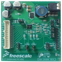
Manufacturer Part Number
KIT34844AEPEVBE
Description
LED Lighting Development Kits IC, 10 CHANNEL LED BACKLIGHT
Manufacturer
Freescale Semiconductor
Datasheet
1.MC34844AEP.pdf
(62 pages)
Specifications of KIT34844AEPEVBE
Supply Voltage
12 V
Supply Current
2 uA
For Use With/related Products
34844A
Lead Free Status / RoHS Status
Lead free / RoHS Compliant


A0/SEN
voltage Protection (OVP) Control.
CURRENT SET (ISET)
current can be set by using a resistor from this pin to GND.
POSITIVE CURRENT SCALING (PIN)
current control. Applying 0 V to this pin, scales the current to
near 0%, and in the same way, applying 2.048 V (Vset), the
scale factor is 100%. By applying a voltage higher than 2.2 V,
the scaling factor is disabled, and the internal pull-ups are
activated.
applying 0 V to the PIN pin and 2.048 V to NIN pin, scales the
current to near 0%, and in the same way, applying 2.048 V to
the PIN pin and 0 V to NIN pin, scales the current to 100%.
By applying a voltage higher than 2.2 V, the scaling factor is
disabled and the internal pull-ups are activated in both pins.
NEGATIVE CURRENT SCALING (NIN)
current control. Setting 0 V to this pin scales the current to
100%, in the same way, setting 2.048 V (Vset) the scale
factor is near 0%. By applying a voltage higher than 2.2 V, the
scaling factor is disabled and the internal pull-ups are
activated.
applying 0 V to the PIN pin and 2.048 V to NIN pin, scales the
current near 0%, and in the same way, applying 2.048 V to
the PIN pin and 0 V to NIN pin, scales the current to 100%.
Address select, device select pin, or Hardware Over-
Each LED string can drive up to 50 mA. The maximum
Positive current scaling factor for the external analog
If PIN pin and NIN pin are used at the same time then by
Negative current scaling factor for the external analog
If PIN pin and NIN pin are used at the same time then by
FUNCTIONAL DESCRIPTION
FUNCTIONAL PIN DESCRIPTION
15
34844
By applying a voltage higher than 2.2 V, the scaling factor is
disabled and the internal pull-ups are activated in both pins.
GROUND (GND)
Boost FET.
dissipation.
I0-I9
up to 50 mA.
FAULT DETECTION PIN (FAIL)
impedance.
BOOST SLOPE COMPENSATION SETTING
RESISTOR (SLOPE)
Boost compensation slope.
POWER GROUND PINS (PGNDA, PGNDB)
OUTPUT VOLTAGE SENSE PIN (VOUT)
input voltage for the internal regulator 2 (VDC2).
SWITCHING NODE PINS (SWA, SWB)
Ground Reference for all internal circuits other than the
The Exposed Pad (EP) should be used for thermal heat
Current LED driver, each line has the capability of driving
When a fault situation is detected, this pin goes into high
Use an external resistor of about 68 kΩ to configure the
Ground pin for the internal Boost FET.
Input pin to monitor the output voltage. It also supplies the
Switching node of boost converter.
Analog Integrated Circuit Device Data
Freescale Semiconductor
Related parts for KIT34844AEPEVBE
Image
Part Number
Description
Manufacturer
Datasheet
Request
R

Part Number:
Description:
Manufacturer:
Freescale Semiconductor, Inc
Datasheet:
Part Number:
Description:
Manufacturer:
Freescale Semiconductor, Inc
Datasheet:
Part Number:
Description:
Manufacturer:
Freescale Semiconductor, Inc
Datasheet:
Part Number:
Description:
Manufacturer:
Freescale Semiconductor, Inc
Datasheet:
Part Number:
Description:
Manufacturer:
Freescale Semiconductor, Inc
Datasheet:
Part Number:
Description:
Manufacturer:
Freescale Semiconductor, Inc
Datasheet:
Part Number:
Description:
Manufacturer:
Freescale Semiconductor, Inc
Datasheet:
Part Number:
Description:
Manufacturer:
Freescale Semiconductor, Inc
Datasheet:
Part Number:
Description:
Manufacturer:
Freescale Semiconductor, Inc
Datasheet:
Part Number:
Description:
Manufacturer:
Freescale Semiconductor, Inc
Datasheet:
Part Number:
Description:
Manufacturer:
Freescale Semiconductor, Inc
Datasheet:
Part Number:
Description:
Manufacturer:
Freescale Semiconductor, Inc
Datasheet:
Part Number:
Description:
Manufacturer:
Freescale Semiconductor, Inc
Datasheet:
Part Number:
Description:
Manufacturer:
Freescale Semiconductor, Inc
Datasheet:
Part Number:
Description:
Manufacturer:
Freescale Semiconductor, Inc
Datasheet: