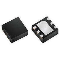
MAX9635ESA+ Maxim Integrated Products, MAX9635ESA+ Datasheet - Page 16

MAX9635ESA+
Manufacturer Part Number
MAX9635ESA+
Description
Optical Sensors - Board Mount LOW-POW AMBIENT LIGHT SENSR W/ADC
Manufacturer
Maxim Integrated Products
Datasheet
1.MAX9635EDTT.pdf
(20 pages)
Specifications of MAX9635ESA+
Supply Current
0.65 uA
Operating Supply Voltage
1.7 V to 3.6 V
Package / Case
uTDFN-6
Maximum Operating Temperature
+ 85 C
Minimum Operating Temperature
- 40 C
Lead Free Status / RoHS Status
Lead free / RoHS Compliant
Industry’s Lowest-Power
Ambient Light Sensor with ADC
Figure 4. START, STOP, and REPEATED START Conditions
The slave address is controlled by the A0 pin. Connect
A0 to either ground or V
shows the two possible addresses for the IC.
The acknowledge bit (ACK) is a clocked 9th bit that the
IC uses to handshake receipt each byte of data when in
write mode (see Figure 5). The IC pulls down SDA dur-
ing the entire master-generated ninth clock pulse if the
previous byte is successfully received. Monitoring ACK
allows for detection of unsuccessful data transfers. An
unsuccessful data transfer occurs if a receiving device
is busy or if a system fault has occurred. In the event of
an unsuccessful data transfer, the bus master can retry
communication. The master pulls down SDA during the
ninth clock cycle to acknowledge receipt of data when
the IC is in read mode. An acknowledge is sent by the
master after each read byte to allow data transfer to
continue. A not acknowledge is sent when the master
reads the final byte of data from the IC, followed by a
STOP condition.
A write to the IC includes transmission of a START condi-
tion, the slave address with the R/W bit set to 0, one byte
of data to configure the internal register address pointer,
one or more bytes of data, and a STOP condition. Figure
6 illustrates the proper frame format for writing one byte
of data to the IC.
Table 10. Slave Address
16
GND
V
A0
SDA
SCL
CC
S
SLAVE ADDRESS
FOR WRITING
0x94
0x96
CC
to set the address. Table 10
SR
Write Data Format
SLAVE ADDRESS
FOR READING
Slave Address
Acknowledge
0x95
0x97
P
Figure 5. Acknowledge
The slave address with the R/W bit set to 0 indicates
that the master intends to write data to the IC. The IC
acknowledges receipt of the address byte during the
master-generated ninth SCL pulse.
The second byte transmitted from the master configures
the IC’s internal register address pointer. The pointer
tells the IC where to write the next byte of data. An
acknowledge pulse is sent by the IC upon receipt of the
address pointer data.
The third byte sent to the IC contains the data that is writ-
ten to the chosen register. The master signals the end of
transmission by issuing a STOP condition.
To read a byte of data, the register pointer must first be
set through a write operation (Figure 7). Send the slave
address with the R/W set to 0, followed by the address
of the register that needs to be read. After a repeated
start condition, send the slave address with the R/W bit
set to 1 to initiate a read operation. The IC then sends
an acknowledge pulse followed by the contents of the
register to be read. Transmitted data is valid on the rising
edge of the master-generated serial clock (SCL).
The photo sensitive area of the IC is 0.37mm x 0.37mm
and much smaller than the device itself. When placing
the part behind a light guide, only this sensitive area has
to be taken into account. Figure 8 shows the position and
size of the photo sensitive area within the package.
PROCESS: BiCMOS
SDA
SCL
CONDITION
START
1
2
Chip Information
NOT ACKNOWLEDGE
ACKNOWLEDGE
Read Data Format
ACKNOWLEDGMENT
8
Sensor Position
CLOCK PULSE FOR
9


