DLP-USB245M DLP Design Inc, DLP-USB245M Datasheet
DLP-USB245M
Specifications of DLP-USB245M


Related parts for DLP-USB245M


DLP-USB245M Summary of contents
Page 1
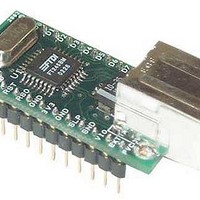
... DLP-USB245M-G USB to FIFO Parallel Interface Module The DLP-USB245M-G is the 2nd generation, lead free version of DLP Design’s USB adapter. This device adds extra functionality to it’s DLP-USB1 predecessor with a reduced component count and a new low price. DLP-USB245M FEATURES • Send / Receive Data over USB Bytes / sec • ...
Page 2
... GENERAL DESCRIPTION The DLP-USB245M provides an easy cost-effective method of transferring data to / from a peripheral and a host Million bits (1-Megabyte) per second. Its simple FIFO-like design makes it easy to interface to any microcontroller or microprocessor via IO ports. To send data from the peripheral to the host computer simply write the byte wide data into the module when TXE# is low ...
Page 3
... Unzip the file to a blank floppy disk or folder on your PC. The drivers can co-exist on the same floppy disk or folder since the INF files determine which set of drivers to load for each operating system version. Once loaded, the VCP drivers allow your application software, running on the host PC, to communicate with the DLP-USB245M as though it were connected to a COM (RS-232) port. ...
Page 4
... Download the serializer program from either dlpdesign.com or ftdichip.com. Unzip the package and place folder on the hard drive. 3. Select a power source for the DLP-USB245M module via pins 10, 11, and 12. Be sure to pull the RESET# pin high (pin 3). 4. Connect the DLP-USB245M board to the PC via a standard, 6-foot USB cable. This action initiates the loading of the USB drivers. When prompted, select the folder where the DLL version of the device drivers were stored Copyright © ...
Page 5
... Terminate the serializer program and disconnect the DLP-USB245M board from the USB cable. Wait 10 seconds and reconnect the DLP-USB245M board. Reboot the PC if instructed to do so. NOTE 1 - The DLP-USB245M comes pre-programmed with a default VID and PID. Step 5 is optional and only required if different VID/PID codes are required. ...
Page 6
... Table 1 - DLP-USB245M PINOUT DESCRIPTION 1 12 Pin# Description 1 BOARD ID (Out) Identifies the board as either a DLP-USB245M or DLP-USB232M. High for DLP- USB232M and low for DLP-USB245M. 2 Ground 3 RESET# (In) Can be used by an external device to reset the FT245BM. If not required this pin must be tied to VCC. 4 RESETO# (Out) Output of the internal Reset Generator. Stays high impedance for ~ 2ms after VCC > ...
Page 7
... SND/WUP (In) If the DLP-USB245M is in USB suspend, a positive edge on this pin (WAKEUP) initiates a remote wakeup sequence. If the device is active (not in suspend) a positive edge on this pin (SEND) causes the data in the write buffer to be sent to the PC on the next USB Data-In request regardless of how many bytes are in the buffer ...
Page 8
... A Bus Powered High Power Device ( one that draws more than 100mA ) should use the SLEEP# pin to keep the current below 100mA on plug-in and 500uA on USB suspend device that consumes more than 100mA can not be plugged into a USB Bus Powered Hub Figure 2 5.0V DLP-USB245M User Manual Microcontroller 8 data WR RD# 3 ...
Page 9
... Figure 3 3.3V Figure 3 shows how to configure the DLP-USB245M to interface with a 3.3v logic device. In this example, the target electronics provides the 3.3 volts via the VCCIO line (pin 10) which in turn will cause the FIFO interface IO pins to drive out at 3.3v level. Bus Powered Circuit with Power Control USB Bus powered circuits need to be able to power down in USB suspend mode in order to meet the < ...
Page 10
... DLP-USB245M TIMING DIAGRAM – FIFO READ CYCLE RXF# RD# T3 D[7..0] D Description Min Max Unit Time Description T1 RD Active Pulse Width Pre-Charge Time T3 RD Active to Valid Data T4 Valid Data Hold Time from RD Inactive T5 RD Inactive to RXF# T6 RXF inactive after RD cycle DLP-USB1 TIMING DIAGRAM – FIFO WRITE CYCLE ...
Page 11
... Inches(millimeters) unless otherwise noted 1.5 typ (38.1 typ) .235 typ (6.0 typ) .50 typ (12.7 typ) .16 typ (4.2 typ) Copyright © DLP Design 2002 DLP-USB245M User Manual .52 typ dia (13.2 typ) .19 typ dia (.46 typ) .6 typ (15.2 typ) .7 typ (17.8 typ) .10 typ (2.54 typ) ...
Page 12
... VHys Input Switching Hysteresis FIFO IO Pin Characteristics ( VCCIO = 3.3v ) Parameter Description Voh Output Voltage High Vol Output Voltage Low Vin Input Switching Threshold VHys Input Switching Hysteresis Copyright © DLP Design 2002 DLP-USB245M User Manual 150 Min Typ Max Units 4.4 5 ...
Page 13
... Differential Common Mode UVDif Differential Input Sensitivity UDrvZ Driver Output Impedance Note 2 – Driver Output Impedance includes the external 27R series resistors on USBDP and USBDM pins. Copyright © DLP Design 2002 DLP-USB245M User Manual Min Typ Max Units 1.1 1.5 1.9 ...
Page 14
... This document provides preliminary information that may be subject to change without notice. Contact Information DLP Design 1605 Roma Lane Allen, TX 75013 Phone: 469-964-8027 Fax: 415-901-4859 Email: support@dlpdesign.com Internet: http://www.dlpdesign.com Copyright © DLP Design 2002 DLP-USB245M User Manual Page ...
Page 15
... Appendix A – DLP USB245M Schematic VCC-IO 13 VCC 26 VCC 3 AVCC 30 Copyright © DLP Design 2002 DLP-USB245M User Manual GND 17 GND 9 AGND 29 GND 5 Page ...