DLP-USB245M DLP Design Inc, DLP-USB245M Datasheet - Page 6
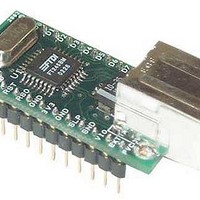
DLP-USB245M
Manufacturer Part Number
DLP-USB245M
Description
Interface Modules & Development Tools USB-FIFO Adapter
Manufacturer
DLP Design Inc
Datasheet
1.DLP-USB245M-G.pdf
(15 pages)
Specifications of DLP-USB245M
Interface Type
USB
Operating Supply Voltage
- 0.5 V to + 6 V
Product
Interface Modules
For Use With/related Products
FT245BM
Lead Free Status / RoHS Status
Lead free / RoHS Compliant


Table 1 - DLP-USB245M PINOUT DESCRIPTION
Pin#
1
2
3
4
5
6
7
8
Description
BOARD ID
USB232M and low for DLP-USB245M.
Ground
RESET#
be tied to VCC.
RESETO#
VCC > 3.5v and the internal clock starts up, then clamps it’s output to the 3.3v output of the internal
regulator. Taking RESET# low will also force RSTOUT# to go high impedance. RSTOUT# is NOT
affected by a USB Bus Reset.
Ground
3V3OUT
internal 3.3v supply to the USB transceiver cell and the RSTOUT# pin. A small amount of current
(<= 5mA ) can be drawn from this pin to power external 3.3v logic if required.
Ground
SLEEP
Can be used to control power to external logic using a P-Channel Logic Level
MOSFET switch.
12
1
Copyright © DLP Design 2002
(Out) Goes Low after the device is configured via USB, then high during USB suspend.
(In) Can be used by an external device to reset the FT245BM. If not required this pin must
(Out) Output from the integrated L.D.O. regulator. It’s primary purpose is to provide the
(Out) Output of the internal Reset Generator. Stays high impedance for ~ 2ms after
(Out) Identifies the board as either a DLP-USB245M or DLP-USB232M. High for DLP-
13
24
DLP-USB245M User Manual
Page 6 of 15
Related parts for DLP-USB245M
Image
Part Number
Description
Manufacturer
Datasheet
Request
R

Part Number:
Description:
Interface Modules & Development Tools USB to MSP430 w/ FTDI FT2232H
Manufacturer:
DLP Design Inc
Datasheet:

Part Number:
Description:
MODULE USB SECURITY DONGLE
Manufacturer:
DLP Design Inc
Datasheet:

Part Number:
Description:
MODULE USB-TO-UART/FIFO HS 18DIP
Manufacturer:
DLP Design Inc
Datasheet:

Part Number:
Description:
MODULE USB ADAPTER FOR FT2232D
Manufacturer:
DLP Design Inc
Datasheet:

Part Number:
Description:
MODULE USB-TO-FPGA TOOL W/MANUAL
Manufacturer:
DLP Design Inc
Datasheet:
Part Number:
Description:
Interface Modules & Development Tools RETRACTABLE USB CBL USB TO MINI USB
Manufacturer:
DLP Design Inc
Part Number:
Description:
Interface Modules & Development Tools USB FPGA Module w/ Xilinx XC3S400A
Manufacturer:
DLP Design Inc
Datasheet:

Part Number:
Description:
MODULE USB-TO-PARL FIFO 18-DIP
Manufacturer:
DLP Design Inc
Datasheet:

Part Number:
Description:
MODULE USB-TO-SRL UART 18-DIP
Manufacturer:
DLP Design Inc
Datasheet:

Part Number:
Description:
MODULE USB ADAPTR FOR FT2232D LP
Manufacturer:
DLP Design Inc
Datasheet:

Part Number:
Description:
MODULE USB-MCU FT245RL W/16F877A
Manufacturer:
DLP Design Inc
Datasheet:

Part Number:
Description:
MODULE USB-TO-FPGA TRAINING TOOL
Manufacturer:
DLP Design Inc
Datasheet:

Part Number:
Description:
MODULE USB-MCU FT232R W/18F2410
Manufacturer:
DLP Design Inc
Datasheet:

Part Number:
Description:
MODULE USB-MCU FT245RL W/SX48
Manufacturer:
DLP Design Inc
Datasheet:

Part Number:
Description:
MODULE USB-MCU FT2232D W/16F877A
Manufacturer:
DLP Design Inc
Datasheet: