EVALA5972D STMicroelectronics, EVALA5972D Datasheet - Page 19
EVALA5972D
Manufacturer Part Number
EVALA5972D
Description
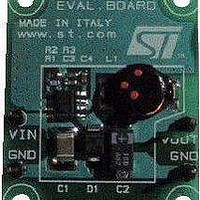
Power Management Modules & Development Tools EVAL BOARD A5972 Auto Grade
Manufacturer
STMicroelectronics
Type
DC/DC Switching Converters, Regulators & Controllersr
Datasheet
1.EVALA5972D.pdf
(29 pages)
Specifications of EVALA5972D
Input Voltage
4.4 V to 36 V
Output Voltage
1.235 V to 35 V
Board Size
23 mm x 20 mm
Product
Power Management Modules
Supply Current
2 A
Dimensions
23 mm x 20 mm
For Use With/related Products
AN1517
Lead Free Status / RoHS Status
Lead free / RoHS Compliant


AN1517
5.3
Thermal considerations
The dissipated power of the device is tie to three different sources:
●
Equation 21
where D is the duty cycle of the application. Note that the duty cycle is theoretically given by
the ratio between V
compensate for the losses of the overall application. For this reason, the switching losses
related to the R
●
Equation 22
Where T
current flowing into it during the turn ON and turn OFF phases. T
switching time.
●
Equation 23
where I
●
R
@ 150 °C. We can consider a value of 0.4 Ω.
T
losses are:
Equation 24
The junction temperature of device will be:
Equation 25
Where T
ambient.
SW
DSON
switch losses due to the not negligible R
Switching losses due to turning ON and OFF. These are derived using the following
equation:
Quiescent current losses.
Example:
–
–
–
is approximately 70 ns. I
Q
has a typical value of 0.25 Ω @ 25 °C and increases up to a maximum value of 0.5 Ω
A
ON
is the quiescent current.
V
V
I
OUT
is the ambient temperature and Rth
IN
OUT
P
and T
SW
P
= 5 V
=
TOT
= 1.5 A
DSON
= 3.3 V
0.4 1.5
=
OFF
V
OUT
⋅
=
IN
increase compared to an ideal case.
are the overlap times of the voltage across the power switch and the
R DSON
•
2
and V
I
⋅
OUT
0.7
Q
+
IN
⋅
•
P
has a typical value of 2.5 mA @ V
5 1.5 70 10
(
, but in practice it is substantially higher than this value to
(
---------------------------------------- -
I OUT
ON
⋅
T
T
ON
J
=
=
⋅
)
+
2
2
P
R
T
T
⋅
Q
DSON
A
OFF
D
⋅
+
=
+
Rth
–
V
V
DSON
)
9
J-A
IN I OUT T SW F SW
IN
•
⋅
•
J A
F
250 10
–
(
⋅
•
is the thermal resistance junction-to-
SW
I
. These are equal to:
OUT
I
Q
•
⋅
P
=
TOT
)
⋅
3
2
V
+
•
IN
D
5 2.5 10
•
⋅
I
⋅
OUT
⋅
SW
IN
Application information
•
= 12 V. The overall
+
–
is the equivalent
T
3
V IN I Q =
SW
≅
0.9W
⋅
•
F
SW
19/29
Related parts for EVALA5972D
Image
Part Number
Description
Manufacturer
Datasheet
Request
R

Part Number:
Description:
ENERCHIP CC EVAL KIT
Manufacturer:
Cymbet Corporation
Datasheet:

Part Number:
Description:
BOARD EVAL FOR AD976
Manufacturer:
Analog Devices Inc
Datasheet:

Part Number:
Description:
BOARD EVAL FOR ADXL345
Manufacturer:
Analog Devices Inc
Datasheet:

Part Number:
Description:
ENERCHIP CC SEH EVAL KIT
Manufacturer:
Cymbet Corporation
Datasheet:

Part Number:
Description:
ENERCHIP EP ENERGY HARVEST EVAL
Manufacturer:
Cymbet Corporation
Datasheet:

Part Number:
Description:
EVAL BOARD FOR TW6864-LB2-GR
Manufacturer:
Intersil
Datasheet:
Part Number:
Description:
EVAL BOARD FOR TW8816-LB3-GR
Manufacturer:
Intersil
Datasheet:
Part Number:
Description:
EVAL BOARD FOR TW8817-TA3-GRS
Manufacturer:
Intersil
Datasheet:

Part Number:
Description:
EVALUATION MODULE FOR ADUM4160
Manufacturer:
Analog Devices Inc
Datasheet:

Part Number:
Description:
BOARD EVALUATION ADCMP581BCP
Manufacturer:
Analog Devices Inc
Datasheet:
Part Number:
Description:
BOARD EVALUATION ADM1041
Manufacturer:
Analog Devices Inc
Datasheet:

Part Number:
Description:
EVAL BOARD FOR STM32F107VCT
Manufacturer:
STMicroelectronics
Datasheet:
Part Number:
Description:
BOARD EVAL FOR AD1954
Manufacturer:
Analog Devices Inc
Datasheet:
Part Number:
Description:
BOARD EVAL FOR AD1955
Manufacturer:
Analog Devices Inc
Datasheet:

Part Number:
Description:
BOARD EVAL FOR AD7655
Manufacturer:
Analog Devices Inc
Datasheet: