EVALA5972D STMicroelectronics, EVALA5972D Datasheet - Page 8
EVALA5972D
Manufacturer Part Number
EVALA5972D
Description
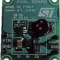
Power Management Modules & Development Tools EVAL BOARD A5972 Auto Grade
Manufacturer
STMicroelectronics
Type
DC/DC Switching Converters, Regulators & Controllersr
Datasheet
1.EVALA5972D.pdf
(29 pages)
Specifications of EVALA5972D
Input Voltage
4.4 V to 36 V
Output Voltage
1.235 V to 35 V
Board Size
23 mm x 20 mm
Product
Power Management Modules
Supply Current
2 A
Dimensions
23 mm x 20 mm
For Use With/related Products
AN1517
Lead Free Status / RoHS Status
Lead free / RoHS Compliant


Functional description
2.5
2.6
8/29
Due to this reduction of the ON time, the output voltage decreases.
Since the minimum switch ON time (necessary to avoid a false over-current signal) is too
short to obtain a sufficiently low duty cycle at 250 kHz, the output current, in strong over-
current or short-circuit conditions, could increase again. For this reason the switching
frequency is also reduced, thus keeping the inductor current under its maximum threshold.
The Frequency Shifter
voltage decreases (due to the reduced duty cycle), the switching frequency decreases also.
Figure 7.
Error amplifier
The voltage error amplifier is the core of the loop regulation. It is a transconductance
operational amplifier whose non inverting input is connected to the internal voltage
reference (1.235 V), while the inverting input (FB) is connected to the external divider or
directly to the output voltage. The output (COMP) is connected to the external compensation
network. The uncompensated error amplifier has the following characteristics:
Table 2.
The error amplifier output is compared with the oscillator sawtooth to perform PWM control.
PWM comparator and power stage
This block compares the oscillator sawtooth and the error amplifier output signals
generating the PWM signal for the driving stage.
The power stage is a highly critical block, as it functions to guarantee a correct turn ON and
turn OFF of the PDMOS. The turn ON of the power element, or more accurately, the rise
time of the current at turn ON, is a very critical parameter. At a first approach, it appears that
Minimum sink/source voltage
Output voltage swing
Low frequency gain
Transconductance
Input bias current
Description
Current limitation circuitry
Uncompensated error amplifier characteristics
A1/A2=95
(Figure
DRIVER
VCC
OUT
I
OFF
6) functions based on the feedback voltage. As the feedback
PWM
A1
RSENSE
A2
I
1500 µA/300 µA
0.4 V/3.65 V
2300 µS
Values
2.5 µA
65 dB
I
NOT
AM00008v1
RTH
I
L
AN1517
Related parts for EVALA5972D
Image
Part Number
Description
Manufacturer
Datasheet
Request
R

Part Number:
Description:
ENERCHIP CC EVAL KIT
Manufacturer:
Cymbet Corporation
Datasheet:

Part Number:
Description:
BOARD EVAL FOR AD976
Manufacturer:
Analog Devices Inc
Datasheet:

Part Number:
Description:
BOARD EVAL FOR ADXL345
Manufacturer:
Analog Devices Inc
Datasheet:

Part Number:
Description:
ENERCHIP CC SEH EVAL KIT
Manufacturer:
Cymbet Corporation
Datasheet:

Part Number:
Description:
ENERCHIP EP ENERGY HARVEST EVAL
Manufacturer:
Cymbet Corporation
Datasheet:

Part Number:
Description:
EVAL BOARD FOR TW6864-LB2-GR
Manufacturer:
Intersil
Datasheet:
Part Number:
Description:
EVAL BOARD FOR TW8816-LB3-GR
Manufacturer:
Intersil
Datasheet:
Part Number:
Description:
EVAL BOARD FOR TW8817-TA3-GRS
Manufacturer:
Intersil
Datasheet:

Part Number:
Description:
EVALUATION MODULE FOR ADUM4160
Manufacturer:
Analog Devices Inc
Datasheet:

Part Number:
Description:
BOARD EVALUATION ADCMP581BCP
Manufacturer:
Analog Devices Inc
Datasheet:
Part Number:
Description:
BOARD EVALUATION ADM1041
Manufacturer:
Analog Devices Inc
Datasheet:

Part Number:
Description:
EVAL BOARD FOR STM32F107VCT
Manufacturer:
STMicroelectronics
Datasheet:
Part Number:
Description:
BOARD EVAL FOR AD1954
Manufacturer:
Analog Devices Inc
Datasheet:
Part Number:
Description:
BOARD EVAL FOR AD1955
Manufacturer:
Analog Devices Inc
Datasheet:

Part Number:
Description:
BOARD EVAL FOR AD7655
Manufacturer:
Analog Devices Inc
Datasheet: