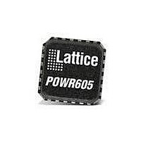
PAC-POWR607-EV Lattice, PAC-POWR607-EV Datasheet - Page 3

PAC-POWR607-EV
Manufacturer Part Number
PAC-POWR607-EV
Description
MCU, MPU & DSP Development Tools ispPAC POWR607 EVAL BRD
Manufacturer
Lattice
Series
ispPAC®r
Specifications of PAC-POWR607-EV
Processor To Be Evaluated
ispPAC-POWR607
Interface Type
JTAG
Maximum Operating Temperature
+ 85 C
Minimum Operating Temperature
- 40 C
Operating Supply Voltage
3.96 V
Core Architecture
CPLD
Main Purpose
Power Management, Power Supply Supervisor/Tracker/Sequencer
Embedded
Yes, Other
Utilized Ic / Part
ispPAC-POWR607
Primary Attributes
-
Secondary Attributes
4.5 ~ 9 V Supply
Lead Free Status / RoHS Status
Lead free / RoHS Compliant
ispPAC-POWR607
Lattice Semiconductor
Evaluation Board User’s Guide
Power Supply Considerations
The ispPAC-POWR607 device operates with analog and digital core power supplies of 3.3V, To simplify evaluation
work, the evaluation board was designed to operate from a single 4.5V to 9V power supply, which may be brought
in through a standard 5mm power plug (J2 - center tip positive). The evaluation board provides a linear regulator to
provide the appropriate operating voltages for the ispPACPOWR607 device, as well as reverse polarity protection.
The kit comes with a battery and cable that plugs into the connector at J2 and provides power with a 9V battery,
see Figure 2. If it is desired to test the current in the power down mode of the ispPAC-POWR607, the link between
pins 3 and 4 of J1 should be cut (please refer to Appendix A). Otherwise, approximately 2mA will be drawn when
the device is in power down mode.
Figure 2. 9V Battery Power Interface
Input/Output Connections
Connectors are provided for key functions and test points on this evaluation board, as shown In Figure 1. The JTAG
programming cable is connected to a header (J3) in the lower right corner of the board.
Access to the ispPAC-POWR607 device’s I/O pins is available along the left edge of the assembly, where a 2x17
block of pads (J1)supports the attachment of test probes or a ribbon-cable connector. In addition, there is an array
of 70 proto-type holes for interfacing.
Two momentary switches, S1 and S2, are provided on the evaluation board. They are connected to IN1_PWRDN
and IN2 respectively. Several LEDs are also provided on the evaluation board to indicate proper function and as
aids to debugging. LED D2 indicates that the on-board 3.3V supply is powered up. LED D3 is connected to the
ispPACPOWR607 device’s TDO line, and will briefly flash when downloading, indicating that download data has
made it to the device. Five LEDs are also provided on digital outputs OUT3 through OUT7 so that a user may easily
view the progress of Sequence, Monitor, Reset programs run on the evaluation board.
Demo Sequence and Reprogramming
This evaluation board is shipped from the factory pre-programmed with the “ispPAC_POWR607_LED_Blinker.PAC”
sequence from PAC-Designer’s library. The IN1_PWRDN button must be depressed in order t bring the ispPAC-
POWR607 device out of its power down mode. The programmed sequence will cause the LEDs to flash for about
six seconds, and then the device will revert to the power down mode.
In order to reprogram the ispPAC-POWR607, it must be brought out of power down mode. Thus, the IN1_PWRDN
button must be depressed immediately before beginning a download to the device from PAC-Designer or ispVM.
3


