4432-DKDB0 Silicon Laboratories Inc, 4432-DKDB0 Datasheet - Page 54
4432-DKDB0
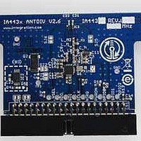
Manufacturer Part Number
4432-DKDB0
Description
WiFi / 802.11 Modules & Development Tools Ant. Diversity 4432 Testcard High band
Manufacturer
Silicon Laboratories Inc
Datasheet
1.SDBC-DK3.pdf
(76 pages)
Specifications of 4432-DKDB0
Modulation
GFSK
Operating Voltage
3.3 V
Antenna
SMA
For Use With/related Products
Si4432
Lead Free Status / RoHS Status
Lead free / RoHS Compliant


SDBC-DK3 UG
The RFIdle() function sets the transceiver and the RF stack into an IDLE state independent of the actual state of
the RF stack. It disables the transmit/receive mode and all the interrupts. It then reads the interrupt status registers
from the radio and clears the IT flags.
The RFTransmit() function starts packet transmission and ensures packets are sent successfully.
The RFReceive() function enables packet reception by enabling the receiver and setting up the relevant interrupts
prior to and reading the interrupt status registers.
The RFPacketReceived() function checks whether the packet is received or not. It reads the data packet from the
FIFO if all packet handlers and the CRC are correct.
54
ChargepumpCT:
============================================================================
// This table contains the modem parameters for different data rates. See the comments for more details
code uint8 RfSettings[NMBR_OF_SAMPLE_SETTING][NMBR_OF_PARAMETER] =
{
// IFBW, COSR, CRO2, CRO1, CRO0, CTG1, CTG0, TDR1, TDR0, MMC1, FDEV,AFC, ChargepumpCT
{0x01, 0x83, 0xc0, 0x13, 0xa9, 0x00, 0x05, 0x13, 0xa9, 0x20, 0x3a, 0x40, 0x80},
{0x04, 0x41, 0x60, 0x27, 0x52, 0x00, 0x0a, 0x27, 0x52, 0x20, 0x48, 0x40, 0x80},
{0x91, 0x71, 0x40, 0x34, 0x6e, 0x00, 0x18, 0x4e, 0xa5, 0x20, 0x48, 0x40, 0x80},
{0x12, 0xc8, 0x00, 0xa3, 0xd7, 0x01, 0x13, 0x51, 0xec, 0x20, 0x13, 0x40, 0x80},
{0x13, 0x64, 0x01, 0x47, 0xAE, 0x04, 0x46, 0xa3, 0xd7, 0x20, 0x13, 0x40, 0x80},
{0x02, 0x64, 0x01, 0x47, 0xae, 0x05, 0x21, 0x0A, 0x3D, 0x00, 0x20, 0x40, 0x80},
{0x05, 0x50, 0x01, 0x99, 0x9A, 0x06, 0x68, 0x0C, 0xCD, 0x00, 0x28, 0x40, 0x80},
{0x9A, 0x3C, 0x02, 0x22, 0x22, 0x07, 0xFF, 0x19, 0x9A, 0x00, 0x50, 0x00,0xC0},
{0x89, 0x5e, 0x01, 0x5D, 0x86, 0x02, 0xAB, 0x20, 0xc5, 0x00, 0x66, 0x00, 0xC0},
};
============================================================================
MMC1:
COSR:
CRO2:
CRO1:
CRO0:
CTG1:
CTG0:
TDR1:
TDR0:
FDEV:
IFBW:
AFC:
Bits
Charge Pump Current Trimming Override
Clock Recovery Oversampling Ratio
Clock Recovery Timing Loop Gain 1
Clock Recovery Timing Loop Gain 1
AFC Loop Gear Shift Override
Modulation Mode Control 1
Clock Recovery Offset 2
Clock Recovery Offset 1
Clock Recovery Offset 0
Frequency Deviation
IF Filter Bandwidth
Register Name
TX Data Rate 1
Table 6. Registers
TX Data Rate 0
Rev. 0.4
//DR: 9.6kbps, DEV: +-45kHz, BBBW:112.8kHz
//DR: 40kbps, DEV: +-20kHz, BBBW: 83.2kHz
//DR: 128kbps, DEV:+-64kHz, BBBW:269.3kHz
//DR: 2.4kbps, DEV:+-36kHz, BBBW: 75.2kHz
//DR: 4.8kbps, DEV: +-45kHz, BBBW: 95.3kHz
//DR: 10kbps, DEV: +-12kHz, BBBW: 41.7kHz
//DR: 20kbps, DEV: +-12kHz, BBBW: 45.2kHz
//DR: 50kbps, DEV: +-25kHz, BBBW:112.8kHz
//DR: 100kbps, DEV: +-50kHz, BBBW: 208 kHz
Register Address
0x1C
0x1D
0x20
0x21
0x22
0x23
0x24
0x25
0x6E
0x6F
0x70
0x72
0x58
// revV2
Related parts for 4432-DKDB0
Image
Part Number
Description
Manufacturer
Datasheet
Request
R

Part Number:
Description:
EZLink Module; F930/4432 Low Band (rev e/B1)
Manufacturer:
Silicon Laboratories Inc
Part Number:
Description:
RF Modules & Development Tools Tx/Rx Split 4432 TRx Testcard
Manufacturer:
Silicon Laboratories Inc
Datasheet:
Part Number:
Description:
RF Modules & Development Tools Sngle Switch Antenna 4432 TRx Testcard
Manufacturer:
Silicon Laboratories Inc
Part Number:
Description:
RF Modules & Development Tools Sngle Switch Antenna 4432 TRx Testcard
Manufacturer:
Silicon Laboratories Inc
Datasheet:
Part Number:
Description:
RF Modules & Development Tools EZLink Module F930/4432 Low Band
Manufacturer:
Silicon Laboratories Inc
Part Number:
Description:
N/A/-40 TO 85 OC/EZLINK MODULE; F930/4432 HIGH BAND (REV E/B1)
Manufacturer:
Silicon Laboratories Inc

Part Number:
Description:
WiFi / 802.11 Modules & Development Tools Single Antenna TRx Testcard Hi band
Manufacturer:
Silicon Laboratories Inc
Datasheet:
Part Number:
Description:
RF Modules & Development Tools Tx/Rx Split 4432 TRx Testcard
Manufacturer:
Silicon Laboratories Inc
Part Number:
Description:
Wireless Accessories EZLink Module F930/4432 High Band
Manufacturer:
Silicon Laboratories Inc

Part Number:
Description:
WiFi / 802.11 Modules & Development Tools Tx/Rx Split 4432 TRx Testcard Hi band
Manufacturer:
Silicon Laboratories Inc
Datasheet:
Part Number:
Description:
Wireless Accessories EZLink Module F930/4432 Low Band
Manufacturer:
Silicon Laboratories Inc
Part Number:
Description:
WiFi / 802.11 Modules & Development Tools Tx/Rx Split TRx Testcard Lw band
Manufacturer:
Silicon Laboratories Inc
Part Number:
Description:
WiFi / 802.11 Modules & Development Tools Single Antenna TRx Testcard Lw band
Manufacturer:
Silicon Laboratories Inc

Part Number:
Description:
SMD/C°/SINGLE-ENDED OUTPUT SILICON OSCILLATOR
Manufacturer:
Silicon Laboratories Inc