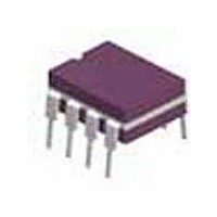
5962-8961501PA National Semiconductor, 5962-8961501PA Datasheet - Page 2

5962-8961501PA
Manufacturer Part Number
5962-8961501PA
Description
EIA/TIA-485/422 DIFF BUS TRANS
Manufacturer
National Semiconductor
Datasheet
1.5962-8961501PA.pdf
(10 pages)
Specifications of 5962-8961501PA
Interface Circuit Standard 1
EIA-422-A/EIA-485
Number Of Receivers
1
Number Of Transmitters
1
Number Of Transceivers
1
Data Transmission Topology
Multipoint
Receiver Signal Type
Differential
Transmitter Signal Type
Differential
Single Supply Voltage (typ)
5V
Single Supply Voltage (min)
4.5V
Single Supply Voltage (max)
5.5V
Dual Supply Voltage (typ)
Not RequiredV
Dual Supply Voltage (min)
Not RequiredV
Dual Supply Voltage (max)
Not RequiredV
Supply Current
28mA
Power Supply Requirement
Single
Operating Temp Range
-55C to 125C
Operating Temperature Classification
Military
Mounting
Through Hole
Pin Count
8
Package Type
CDIP
Lead Free Status / Rohs Status
Not Compliant
Available stocks
Company
Part Number
Manufacturer
Quantity
Price
Company:
Part Number:
5962-8961501PA
Manufacturer:
N/A
Quantity:
1 000
Company:
Part Number:
5962-8961501PA
Manufacturer:
N/A
Quantity:
6 000
Company:
Part Number:
5962-8961501PA
Manufacturer:
NSC
Quantity:
40
www.national.com
V
V
V
V
V
|V
|V
V
Δ|V
I
I
I
I
I
I
O
IH
IL
OS
CC
CCX
Symbol
IH
IL
OH
OL
IC
OC
Δ|V
OD1
OD2
Absolute Maximum Ratings
Specifications for the 883 version of this product are list-
ed separately on the following pages.
Recommended Operating
Conditions
Driver Electrical Characteristics
Over recommended supply voltage and operating temperature ranges, unless otherwise specified
Supply Voltage (V
Storage Temperature Range
Lead Temperature
Maximum Package Power Dissipation
Supply Voltage
Input Voltage (Bus Terminal)
Enable Input Voltage
OC
DS36F95
(Soldering, 60 sec.)
'J' Package
'M' Package
|
|
OD
|
|
Input Voltage HIGH
Input Voltage LOW
Output Voltage HIGH
Output Voltage LOW
Input Clamp Voltage
Differential Output Voltage
Differential Output Voltage
Change in Magnitude of
Differential Output Voltage
(Note
Common Mode Output Voltage
(Note
Change in Magnitude of Common
Mode Output Voltage
Output Current
(Includes Receiver I
Input Current HIGH
Input Current LOW
Short Circuit Output Current
10)
Supply Current
(Total Package)
5)
6)
CC
)
Parameter
(Note
I
)
9)
(Note
4.75
Min Typ Max
9629 Version 12 Revision 6
5)
(Note
5.0 5.25
(Note
−65°C to +175°C
1) at 25°C
I
I
I
I
R
R
R
Figure 1
Output Disabled
V
V
V
V
V
V
No Load,
All Inputs Open
OH
OL
I
O
L
L
L
I
I
O
O
O
O
= −18 mA
(Note
+15V/−10V
= 0 mA
= 2.4V
= 0.4V
= 100Ω,
= 54Ω,
= 54Ω or 100Ω,
= 55 mA
= −7.0V
= 0V
= V
= +12V
= −55 mA
1300 mW
735 mW
Units
CC
300°C
2)
V
7.0V
5.5V
(Note
Figure 1
Figure 1
3,
Print Date/Time: 2009/12/15 10:38:00
2
Conditions
Note
Note 1: Derate 'J' package 8.7 mW/°C above 25°C.
Derate 'M' package 5.88 mW/°C above 25°C.
Voltage at Any Bus Terminal
Differential Input
Output Current HIGH (I
Output Current LOW (I
Operating Temperature (T
4)
0°C to +70°C
0°C to +70°C
−40°C to +125°C
−55°C to +125°C
V
V
DE = 2V, RE = 0.8V
Outputs Enabled
DE = 0.8V, RE = 2V
Outputs Disabled
DS16F95
(Separately or Common Mode)
(V
Voltage (V
Driver
Receiver
Driver
Receiver
DS36F95
DS16F95
O
O
I
= +12V
= −7.0V
or V
CM
)
ID
)
OL
OH
)
)
A
)
Min
2.0
3.0
2.0
1.5
4.50
−7.0
Min Typ Max
−55
0
2.25
Typ
2.0
+25 +70
+25 +125
5.0 5.50
−400
+12
±12
−60
60
16
−250
−150
Max
−1.3
±0.2
±0.4
±0.2
−0.8
−50
150
250
0.8
2.0
6.0
3.0
1.0
20
28
25
Units
mA
mA
mA
μA
°C
°C
V
V
V
Units
mA
mA
mA
μA
μA
V
V
V
V
V
V
V
V
V
V


