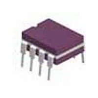
5962-8961501PA National Semiconductor, 5962-8961501PA Datasheet - Page 3

5962-8961501PA
Manufacturer Part Number
5962-8961501PA
Description
EIA/TIA-485/422 DIFF BUS TRANS
Manufacturer
National Semiconductor
Datasheet
1.5962-8961501PA.pdf
(10 pages)
Specifications of 5962-8961501PA
Interface Circuit Standard 1
EIA-422-A/EIA-485
Number Of Receivers
1
Number Of Transmitters
1
Number Of Transceivers
1
Data Transmission Topology
Multipoint
Receiver Signal Type
Differential
Transmitter Signal Type
Differential
Single Supply Voltage (typ)
5V
Single Supply Voltage (min)
4.5V
Single Supply Voltage (max)
5.5V
Dual Supply Voltage (typ)
Not RequiredV
Dual Supply Voltage (min)
Not RequiredV
Dual Supply Voltage (max)
Not RequiredV
Supply Current
28mA
Power Supply Requirement
Single
Operating Temp Range
-55C to 125C
Operating Temperature Classification
Military
Mounting
Through Hole
Pin Count
8
Package Type
CDIP
Lead Free Status / Rohs Status
Not Compliant
Available stocks
Company
Part Number
Manufacturer
Quantity
Price
Company:
Part Number:
5962-8961501PA
Manufacturer:
N/A
Quantity:
1 000
Company:
Part Number:
5962-8961501PA
Manufacturer:
N/A
Quantity:
6 000
Company:
Part Number:
5962-8961501PA
Manufacturer:
NSC
Quantity:
40
t
t
t
t
t
t
t
t
t
t
V
V
V
V
V
V
V
V
I
I
I
I
R
I
I
I
DD
TD
PLH
PHL
ZH
ZL
HZ
LZ
LZL
SKEW
OZ
I
IH
IL
OS
CC
CCX
Symbol
TH
TL
T+
IH
IL
IC
OH
OL
I
Driver Switching Characteristics
V
Symbol
Receiver Electrical Characteristics
Over recommended supply voltage and operating temperature ranges, unless otherwise specified
−V
CC
T−
= 5.0V, T
Differential Input High
Threshold Voltage
Differential Input Low
Threshold Voltage
Hysteresis
Enable Input Voltage HIGH
Enable Input Voltage LOW
Enable Input Clamp Voltage
Output Voltage HIGH
Output Voltage LOW
High Impedance State Output
Line Input Current
Enable Input Current HIGH
Enable Input Current LOW
Input Resistance
Short Circuit Output Current
Supply Current
(Total Package)
Differential Output Delay Time
Differential Output Transition Time
Propagation Delay Time,
Low-to-High Level Output
Propagation Delay Time,
High-to-Low Level Output
Output Enable Time to High Level
Output Enable Time to Low Level
Output Disable Time from High Level
Output Disable Time from Low Level
Output Disable Time from Low Level
with Load Resistor to GND
Skew (Pulse Width Distortion)
A
= 25°C
(Note
Parameter
8)
(Note
(Note
Parameter
9)
7)
9629 Version 12 Revision 6
V
V
V
I
V
I
Figure 2
V
Figure 2
V
Other Input = 0V
V
V
(Note 9)
No Load,
All Inputs Open
I
OH
O
O
CM
ID
ID
O
IH
IL
= −18 mA
= 2.7V, I
= 0.5V, I
= 0.4V to 2.4V
= 0.4V
= −400 μA,
= 200 mV,
= −200 mV,
= 2.7V
= 0V
O
O
R
R
R
R
R
R
Load per
Timing per
R
= −0.4 mA
= 8.0 mA
L
L
L
L
L
L
L
Print Date/Time: 2009/12/15 10:38:00
= 60Ω,
= 27Ω,
= 110Ω,
= 110Ω,
= 110Ω,
= 110Ω,
= 60Ω,
3
Conditions
Conditions
Figure 5
Figure 3
Figure 4
Figure 3
Figure 6
Figure 5
Figure 6
Figure 5
Figure 6
0°C to +70°C
I
I
V
V
DE = 2V, RE = 0.8V
Outputs Enabled
DE = 0.8V, RE = 2V
Outputs Disabled
OL
OL
I
I
= +12V
= −7.0V
= 8.0 mA
= 16 mA
−55°C to +125°C
Min
8.0
8.0
6.0
6.0
−0.2
Min
−15
2.0
2.8
2.5
35
14
Typ
300
1.0
15
15
12
12
25
25
20
20
Typ
50
18
Max
4.0
20
22
16
16
32
32
25
25
Max
−1.3
0.45
0.50
±20
−50
−85
0.2
0.8
1.0
0.8
20
22
28
25
www.national.com
Units
Units
ns
ns
ns
ns
ns
ns
ns
ns
ns
ns
mV
mA
mA
mA
μA
μA
μA
kΩ
V
V
V
V
V
V
V


