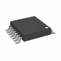
AD5293BRUZ-50 Analog Devices Inc, AD5293BRUZ-50 Datasheet - Page 4

AD5293BRUZ-50
Manufacturer Part Number
AD5293BRUZ-50
Description
1024 Tap, 1% DigiPOT With SPI Interface
Manufacturer
Analog Devices Inc
Datasheet
1.AD5293BRUZ-20.pdf
(24 pages)
Specifications of AD5293BRUZ-50
Taps
1024
Resistance (ohms)
50K
Number Of Circuits
1
Temperature Coefficient
35 ppm/°C Typical
Interface
SPI Serial
Voltage - Supply
9 V ~ 33 V, ±9 V ~ 16.5 V
Operating Temperature
-40°C ~ 105°C
Mounting Type
Surface Mount
Package / Case
14-TSSOP
Resistance In Ohms
50K
Number Of Elements
1
# Of Taps
1024
Resistance (max)
50KOhm
Power Supply Requirement
Single/Dual
Interface Type
Serial (4-Wire/SPI)
Single Supply Voltage (typ)
15V
Dual Supply Voltage (typ)
±15V
Single Supply Voltage (max)
33V
Dual Supply Voltage (max)
±16.5V
Operating Temp Range
-40C to 105C
Operating Temperature Classification
Industrial
Mounting
Surface Mount
Pin Count
14
Lead Free Status / RoHS Status
Lead free / RoHS Compliant
Memory Type
-
Lead Free Status / Rohs Status
Compliant
Available stocks
Company
Part Number
Manufacturer
Quantity
Price
Part Number:
AD5293BRUZ-50
Manufacturer:
ADI/亚德诺
Quantity:
20 000
AD5293
Parameter
DYNAMIC CHARACTERISTICS
1
2
3
4
5
6
7
8
RESISTOR PERFORMANCE MODE CODE RANGE—20 kΩ VERSIONS
Table 2.
Resistor
Tolerance
per Code
1% R-Tolerance
2% R-Tolerance
3% R-Tolerance
Typicals represent average readings at 25°C; V
Resistor position nonlinearity error. R-INL is the deviation from an ideal value measured between R
Code 0x000. R-DNL measures the relative step change from ideal between successive tap positions. The specification is guaranteed in resistor performance mode with
a wiper current of 1 mA for V
The terms resistor performance mode and R-perf mode are used interchangeably.
Guaranteed by design; not subject to production test.
INL and DNL are measured at V
of ±1 LSB maximum are guaranteed monotonic operating conditions.
The A, B, and W resistor terminals have no limitations on polarity with respect to each other. Dual-supply operation enables ground-referenced bipolar signal
adjustment.
P
All dynamic characteristics use V
DISS
Bandwidth
Total Harmonic Distortion
V
Resistor Noise Density
W
is calculated from (I
Settling Time
R
From 0x15E
to 0x3FF
From 0x8C
to 0x3FF
From 0x5A
to 0x3FF
|V
WB
DD
DD
× V
A
− V
DD
< 12 V and 1.2 mA for V
W
) + (I
DD
with the RDAC configured as a potentiometer divider similar to a voltage output DAC. V
4, 8
SS
= +15 V, V
| = 30 V to 33 V
SS
× V
R
From 0x000
to 0x2A1
From 0x000
to 0x373
From 0x000
to 0x3A5
SS
WA
) + (I
SS
DD
= −15 V, and V
LOGIC
Symbol
BW
THD
t
e
S
= +15 V, V
N_WB
× V
W
A
LOGIC
≥ 12 V.
SS
).
R
From 0x1F4
to 0x3FF
From 0xB4
to 0x3FF
From 0x64
to 0x3FF
= −15 V, and V
WB
|V
LOGIC
DD
= 5 V.
− V
SS
Conditions
−3 dB
V
V
band, initial code = zero scale
Code = full scale, R-normal mode
Code = full scale, R-perf mode
Code = half scale, R-normal mode
Code = half scale, R-perf mode
R
0 kHz to 200 kHz
Rev. D | Page 4 of 24
| = 26 V to 30 V
A
A
WB
LOGIC
= 1 V rms, V
= 30 V, V
= 10 kΩ, T
R
From 0x000
to 0x20B
From 0x000
to 0x34B
From 0x000
to 0x39B
= 5 V.
WA
B
= 0 V, ±0.5 LSB error
R
A
AB
B
= 25°C,
= 0 V, f = 1 kHz,
= 20 kΩ
R
From 0x1F4
to 0x3FF
From 0xFA
to 0x3FF
From 0x78
to 0x3FF
WB
WB
|V
at Code 0x00B to Code 0x3FF or between R
DD
− V
SS
| = 22 V to 26 V
R
From 0x000
to 0x20B
From 0x000
to 0x305
From 0x000
to 0x387
Min
WA
A
= V
DD
and V
Typ
520
−93
750
2.5
2.5
5
10
B
R
N/A
From 0xFA
to 0x3FF
From 0x78
to 0x3FF
= 0 V. DNL specification limits
|V
WB
1
DD
− V
Max
WA
SS
at Code 0x3F3 to
| = 21 V to 22 V
R
N/A
From 0x000
to 0x305
From 0x000
to 0x387
WA
Unit
kHz
dB
ns
μs
μs
μs
nV/√Hz


