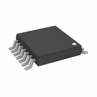
AD5293BRUZ-50 Analog Devices Inc, AD5293BRUZ-50 Datasheet - Page 7

AD5293BRUZ-50
Manufacturer Part Number
AD5293BRUZ-50
Description
1024 Tap, 1% DigiPOT With SPI Interface
Manufacturer
Analog Devices Inc
Datasheet
1.AD5293BRUZ-20.pdf
(24 pages)
Specifications of AD5293BRUZ-50
Taps
1024
Resistance (ohms)
50K
Number Of Circuits
1
Temperature Coefficient
35 ppm/°C Typical
Interface
SPI Serial
Voltage - Supply
9 V ~ 33 V, ±9 V ~ 16.5 V
Operating Temperature
-40°C ~ 105°C
Mounting Type
Surface Mount
Package / Case
14-TSSOP
Resistance In Ohms
50K
Number Of Elements
1
# Of Taps
1024
Resistance (max)
50KOhm
Power Supply Requirement
Single/Dual
Interface Type
Serial (4-Wire/SPI)
Single Supply Voltage (typ)
15V
Dual Supply Voltage (typ)
±15V
Single Supply Voltage (max)
33V
Dual Supply Voltage (max)
±16.5V
Operating Temp Range
-40C to 105C
Operating Temperature Classification
Industrial
Mounting
Surface Mount
Pin Count
14
Lead Free Status / RoHS Status
Lead free / RoHS Compliant
Memory Type
-
Lead Free Status / Rohs Status
Compliant
Available stocks
Company
Part Number
Manufacturer
Quantity
Price
Part Number:
AD5293BRUZ-50
Manufacturer:
ADI/亚德诺
Quantity:
20 000
INTERFACE TIMING SPECIFICATIONS
V
Table 5.
Parameter
t
t
t
t
t
t
t
t
t
t
t
t
t
t
t
t
t
t
1
2
3
4
5
1
2
3
4
5
6
7
8
9
10
11
12
12
12
13
14
RESET
POWER-UP 5
All input signals are specified with t
Maximum SCLK frequency = 50 MHz.
Refer to t
R
Typical power supply voltage slew-rate of 2 V/ms.
2
DD
PULL_UP
4
4
4
4
4
4
4
= V
= 2.2 kΩ to V
SS
12
= ±15 V, V
and t
13
for RDAC register commands operations.
LOGIC
Limit
20
10
10
10
5
5
1
400
14
1
40
2.4
410
1.5
450
450
20
2
LOGIC
with a capacitance load of 168 pF.
3
1
0
= 2.7 V to 5.5 V, and −40°C < T
R
0
Unit
ns min
ns min
ns min
ns min
ns min
ns min
ns min
ns min
ns min
ns min
ns max
μs max
ns max
ms max
ns max
ns max
ns min
ms max
= t
F
= 1 ns/V (10% to 90% of V
C3
CONTROL BITS
C2
Test Conditions/Comments
SCLK cycle time
SCLK high time
SCLK low time
SYNC to SCLK falling edge setup time
Data setup time
Data hold time
SCLK falling edge to SYNC rising edge
Minimum SYNC high time
SYNC rising edge to next SCLK fall ignored
RDY rise to SYNC falling edge
SYNC rise to RDY fall time
RDY low time, RDAC register write command execute time (resistor performance mode)
RDY low time, RDAC register write command execute time (normal mode)
Software\hardware reset
RDY low time, RDAC register read command execute time
SCLK rising edge to SDO valid
Minimum RESET pulse width (asynchronous)
Power-on time to half scale
C1
C0
DD
Figure 2. Shift Register Contents
DB9 (MSB)
A
) and timed from a voltage level of (V
D9
< +105°C. All specifications T
Rev. D | Page 7 of 24
D8
D7
D6
DATA BITS
D5
D4
IL
MIN
+ V
IH
D3
to T
)/2.
MAX
D2
, unless otherwise noted.
D1
DB0 (LSB)
D0
AD5293


