AD7821KPZ Analog Devices Inc, AD7821KPZ Datasheet - Page 2
AD7821KPZ
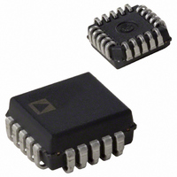
Manufacturer Part Number
AD7821KPZ
Description
8-BIT ATC CONVERTER IC
Manufacturer
Analog Devices Inc
Datasheet
1.AD7821KRZ-REEL.pdf
(16 pages)
Specifications of AD7821KPZ
Number Of Bits
8
Sampling Rate (per Second)
1M
Data Interface
Parallel
Number Of Converters
3
Power Dissipation (max)
50mW
Voltage Supply Source
Dual ±
Operating Temperature
-40°C ~ 85°C
Mounting Type
Surface Mount
Package / Case
20-LCC (J-Lead)
Lead Free Status / RoHS Status
Lead free / RoHS Compliant
Available stocks
Company
Part Number
Manufacturer
Quantity
Price

Company:
Part Number:
AD7821KPZ
Manufacturer:
Analog Devices Inc
Quantity:
10 000
Company:
Part Number:
AD7821KPZ-REEL
Manufacturer:
Analog Devices Inc
Quantity:
10 000


V
apply for RD Mode (Pin 7 = 0 V).
Parameter
UNIPOLAR INPUT RANGE
BIPOLAR INPUT RANGE
REFERENCE INPUT
ANALOG INPUT
LOGIC INPUTS
LOGIC OUTPUTS
POWER SUPPLY
NOTES
1
2
3
4
5
Specifications subject to change without notice.
AD7821–SPECIFICATIONS
Temperature Ranges are as follows: K Version = –40°C to +85°C; B Version = –40°C to +85°C; T Version = –55°C to +125°C.
1 LSB = 19.53 mV for both the unipolar (0 V to +5 V) and bipolar (–2.5 V to +2.5 V) input ranges.
See Terminology.
Sample tested at +25°C to ensure compliance.
See Typical Performance Characteristics.
REF
Resolution
Total Unadjusted Error
Minimum Resolution for which
Resolution
Zero Code Error
Full Scale Error
Signal-to-Noise Ratio (SNR)
Total Harmonic Distortion (THD)
Peak Harmonic or Spurious Noise
Intermodulation Distortion (IMD)
Slew Rate, Tracking
Input Resistance
V
V
Input Voltage Range
Input Leakage Current
Input Capacitance
CS, WR, RD
MODE
DB0–DB7, OFL, INT
Output Capacitance
RDY
I
I
Power Dissipation
Power Supply Sensitivity
DD
SS
(–) = –2.5 V. These test conditions apply unless otherwise stated. All specifications T
REF
REF
No Missing Codes are Guaranteed
V
V
I
I
I
Input Capacitance
V
V
I
I
Input Capacitance
V
V
I
V
I
Output Capacitance
5
INH
INH
INL
INH
INL
OUT
OUT
INH
INL
INH
INL
OH
OL
OL
(+) Input Voltage Range
(–) Input Voltage Range
(CS, RD)
(WR)
(DB0–DB7)
2
2
4
3
4
4
(DB0–DB7)
4
3
3
3
3
3
K Version
8
± 1
8
8
± 1
± 1
45
–50
–50
–50
–50
1.6
2.36
1.0/4.0
V
V
V
± 3
55
2.4
0.8
1
3
–1
8
3.5
1.5
200
–1
8
4.0
0.4
± 3
8
0.4
± 3
8
20
100
50
± 1/4
REF
SS
REF
/V
(–)/V
(–)/V
REF
(+)
DD
REF
1
(+)
B, T Versions
8
± 1
8
8
± 1
± 1
45
–50
–50
–50
–50
1.6
2.36
1.0/4.0
V
V
V
± 3
55
2.4
0.8
1
3
–1
8
3.5
1.5
200
–1
8
4.0
0.4
± 3
8
0.4
± 3
8
20
100
50
± 1/4
REF
SS
REF
/V
(–)/V
(–)/V
REF
V
V
DD
REF
(+)
DD
REF
= +5 V
(–) = GND. Bipolar Input Range: V
(+)
Unit
Bits
LSB max
Bits
Bits
LSB max
LSB max
dB min
dB max
dB max
dB max
dB max
V/µs max
V/µs typ
kΩ min/kΩ max
V min/V max
V min/V max
V min/ max
µA max
pF typ
V min
V max
µA max
µA max
µA max
pF max
V min
V max
µA max
µA max
pF max
V min
V max
µA max
pF max
V max
µA max
pF max
mA max
µA max
mW typ
LSB max
–2–
5%, GND = 0 V. Unipolar Input Range: V
Comments
V
V
V
fa (84.72 kHz) and fb (94.97 kHz) Full-Scale Sine Waves
with f
Second Order Terms
Third Order Terms
–5 V ≤ V
Typically 5 pF
50 µA typ
Typically 5 pF
I
I
Floating State Leakage
Typically 5 pF
I
Floating State Leakage
Typically 5 pF
CS = RD = 0 V
CS = RD = 0 V
± 1/16 LSB typ, V
(V
SOURCE
SINK
SINK
IN
IN
IN
REF
MIN
= 99.85 kHz Full-Scale Sine Wave with f
= 99.85 kHz Full-Scale Sine Wave with f
= 99.85 kHz Full-Scale Sine Wave with f
= 1.6 mA
= 2.6 mA
(+) = 4.75 V max for Unipolar Mode)
SAMPLING
to T
= 360 µA
IN
SS
≤ +5 V
MAX
= –5 V
= 500 kHz
unless otherwise noted. Specifications
DD
= 4.75 V to 5.25 V,
5%, V
SS
REF
= GND, V
(+) = 2.5 V,
REF
SAMPLING
SAMPLING
SAMPLING
(+) = 5 V,
= 500 kHz
= 500 kHz
= 500 kHz
REV. B
Related parts for AD7821KPZ
Image
Part Number
Description
Manufacturer
Datasheet
Request
R

Part Number:
Description:
±1.7g Dual-Axis IMEMS Accelerometer Evaluation Board
Manufacturer:
Analog Devices Inc
Datasheet:

Part Number:
Description:
Inertial Sensor Evaluation System
Manufacturer:
Analog Devices Inc
Datasheet:
Part Number:
Description:
Manufacturer:
Analog Devices Inc
Datasheet:
Part Number:
Description:
Manufacturer:
Analog Devices Inc
Datasheet:
Part Number:
Description:
Manufacturer:
Analog Devices Inc
Datasheet:
Part Number:
Description:
Manufacturer:
Analog Devices Inc
Datasheet:
Part Number:
Description:
Manufacturer:
Analog Devices Inc
Datasheet:
Part Number:
Description:
Manufacturer:
Analog Devices Inc
Datasheet:
Part Number:
Description:
Manufacturer:
Analog Devices Inc
Datasheet:
Part Number:
Description:
Manufacturer:
Analog Devices Inc
Datasheet:
Part Number:
Description:
Manufacturer:
Analog Devices Inc
Datasheet:
Part Number:
Description:
Manufacturer:
Analog Devices Inc
Datasheet:
Part Number:
Description:
Manufacturer:
Analog Devices Inc
Datasheet: