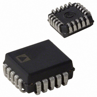
AD7821KPZ Analog Devices Inc, AD7821KPZ Datasheet - Page 7

AD7821KPZ
Manufacturer Part Number
AD7821KPZ
Description
8-BIT ATC CONVERTER IC
Manufacturer
Analog Devices Inc
Datasheet
1.AD7821KRZ-REEL.pdf
(16 pages)
Specifications of AD7821KPZ
Number Of Bits
8
Sampling Rate (per Second)
1M
Data Interface
Parallel
Number Of Converters
3
Power Dissipation (max)
50mW
Voltage Supply Source
Dual ±
Operating Temperature
-40°C ~ 85°C
Mounting Type
Surface Mount
Package / Case
20-LCC (J-Lead)
Lead Free Status / RoHS Status
Lead free / RoHS Compliant
Available stocks
Company
Part Number
Manufacturer
Quantity
Price
Company:
Part Number:
AD7821KPZ
Manufacturer:
Analog Devices Inc
Quantity:
10 000
Company:
Part Number:
AD7821KPZ-REEL
Manufacturer:
Analog Devices Inc
Quantity:
10 000
REV. B
CIRCUIT INFORMATION
BASIC DESCRIPTION
The AD7821 uses a half flash conversion technique (see Func-
tional Block Diagram), whereby two 4-bit flash ADCs are used to
achieve an 8-bit result. Each 4-bit flash ADC contains 15
comparators, which compare an unknown input voltage to the
reference ladder, to achieve a 4-bit result. The MS (most signifi-
cant) flash ADC converts an unknown analog input voltage (V
to provide the 4 MS data bits. An internal DAC, driven by the 4 MS
data bits, then recreates an analog approximation of the input
voltage. The DAC output voltage is subtracted from the analog
input, and the difference is converted by the LS (least significant)
ADC to provide the 4 LS data bits. The MS flash ADC also has one
additional comparator to detect over-range on the analog input.
OPERATING SEQUENCE
The AD7821 has two operating modes. The RD mode allows a con-
version to be started and data to be read with a single, extended,
READ operation (i.e., CS and RD are taken low). The conversion
process is timed out by internal one-shots. The WR-RD mode uses
WR to start a conversion and RD to read the data and allows the
conversion timing to be externally controlled. The operating sequence
for the WR-RD mode is shown in Figure 3.
A conversion is initiated and the analog input signal (V
on the falling edge of WR (falling edge of RD, RD mode). A setup
time (t
prior to this falling edge. See the Digital Interface section for more
details. When WR is low, the internal MS (most significant) ADC
compares the sampled analog input with the reference ladder to
provide the 4 MS data bits. A minimum of 250 ns is required for
this comparison. On the rising edge of WR, the MS data result is
latched internally and the LS (least significant) conversion begins,
to yield the 4 LS data bits. INT goes low typically 380 ns after the
rising edge of WR. This indicates the LS conversion is complete
and that both the LS and MS data results are latched into the
output buffer. RD going low then enables the output data. If a
faster conversion time is required, the RD line can be brought low
250 ns after WR goes high. This latches both the LS and MS
data bits and outputs the conversion result on DB0–DB7.
REFERENCE AND INPUT
The V
fully differential and define the zero and full-scale input range of
the ADC. The transfer characteristic of the part is defined by
the integer value of the following expression:
REF
P
Figure 3. Operating Sequence (WR-RD Mode)
, delay time between conversions) of 350 ns is required
Data (LSBs ) = 256
(–) and V
REF
(+) reference inputs on the AD7821 are
V
REF
V
IN
(+) − V
− V
REF
REF
(−)
(−)
+ 0.5
IN
) sampled
IN
)
–7–
As a result, the analog input (V
up to provide both unipolar and bipolar operation. The data
output code for unipolar and bipolar operation is Natural Binary
and Offset Binary, respectively.
The span of the analog input voltage can easily be varied. By
reducing the reference span, V
the sensitivity of the converter can be increased (i.e., if V
then 1 LSB = 7.8 mV). The reference flexibility also allows the
input span for unipolar operation to be offset from zero (V
GND). Additionally, the input/reference arrangement facilitates
ratiometric operation.
Figures 4 and 5 show some configurations that are possible. For
minimum noise, a 47 µF capacitor in parallel with a 0.1 µF ca-
pacitor should be connected between the reference inputs and
GND.
INPUT CURRENT
The analog input of the AD7821 behaves somewhat differently
than conventional ADCs. This is due to the ADC’s sampled
data comparators, which take varying amounts of input current
depending on the cycle of the converter.
The equivalent input circuit of the AD7821 is shown in Figure 6.
When a conversion ends (e.g., falling edge of INT, WR-RD
mode, t
connected to the comparators of the internal LS and MS ADCs.
Therefore, V
of 1 pF each.
RD
Figure 4. Power Supply as Reference;
Unipolar Operation (0 to + 5 V)
> t
Figure 5. External Reference;
Bipolar Operation (–2.5 V to +2.5 V)
IN
INTL
is simultaneously connected to 31 input capacitors
) all the input switches are closed and V
REF
IN
(+) – V
) of the device can easily be set
REF
(–), to less than 5 V,
AD7821
REF
REF
= 2 V
IN
(–) >
is


