AD8153ACPZ-RL7 Analog Devices Inc, AD8153ACPZ-RL7 Datasheet - Page 19

AD8153ACPZ-RL7
Manufacturer Part Number
AD8153ACPZ-RL7
Description
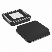
IC,Telecom Switching Circuit,LLCC,32PIN,PLASTIC
Manufacturer
Analog Devices Inc
Series
XStream™r
Datasheet
1.AD8153ACPZ.pdf
(24 pages)
Specifications of AD8153ACPZ-RL7
Applications
2:1 Multiplexer/1:2 De-Multiplexer
Interface
I²C
Voltage - Supply
3 V ~ 3.6 V
Package / Case
32-LFCSP
Mounting Type
Surface Mount
Lead Free Status / RoHS Status
Lead free / RoHS Compliant
For Use With
AD8153-EVALZ - BOARD EVALUATION FOR AD8153
Lead Free Status / RoHS Status
Lead free / RoHS Compliant
Other names
AD8153ACPZ-RL7TR
Available stocks
Company
Part Number
Manufacturer
Quantity
Price
Part Number:
AD8153ACPZ-RL7
Manufacturer:
ADI/亚德诺
Quantity:
20 000
PCB DESIGN GUIDELINES
Proper RF PCB design techniques must be used for optimal
performance.
Power Supply Connections and Ground Planes
Use of one low impedance ground plane is recommended. The
VEE pins should be soldered directly to the ground plane to
reduce series inductance. If the ground plane is an internal
plane and connections to the ground plane are made through
vias, multiple vias can be used in parallel to reduce the series
inductance. The exposed pad should be connected to the VEE
plane using plugged vias so that solder does not leak through
the vias during reflow.
Use of a 10 μF electrolytic capacitor between VCC and VEE is
recommended at the location where the 3.3 V supply enters the
PCB. It is recommended that 0.1 μF and 1 nF ceramic chip
capacitors be placed in parallel at each supply pin for high
frequency power supply decoupling. When using 0.1 μF and 1 nF
ceramic chip capacitors, they should be placed between the IC
power supply pins (VCC, VTTI, VTTO) and VEE, as close as
possible to the supply pins.
By using adjacent power supply and GND planes, excellent high
frequency decoupling can be realized by using close spacing
between the planes. This capacitance is given by
where:
ε
A is the area of the overlap of power and GND planes (cm
d is the separation between planes (mm).
For FR4, ε
r
is the dielectric constant of the PCB material.
C
PLANE
r
= 0.88ε
= 4.4 and 0.25 mm spacing, C ~15 pF/cm
r
A/d (pF)
2
.
2
).
Rev. 0 | Page 19 of 24
Transmission Lines
Use of 50 Ω transmission lines is required for all high frequency
input and output signals to minimize reflections. It is also
necessary for the high speed pairs of differential input traces to
be matched in length, as well as the high speed pairs of differential
output traces, to avoid skew between the differential traces.
Soldering Guidelines for Chip Scale Package
The lands on the 32-lead LFCSP are rectangular. The printed
circuit board pad for these should be 0.1 mm longer than the
package land length and 0.05 mm wider than the package land
width. The land should be centered on the pad. This ensures
that the solder joint size is maximized. The bottom of the chip
scale package has a central exposed pad. The pad on the printed
circuit board should be at least as large as this exposed pad. The
user must connect the exposed pad to VEE using plugged vias
so that solder does not leak through the vias during reflow. This
ensures a solid connection from the exposed pad to VEE.
AD8153


