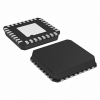
AD8153ACPZ-RL7 Analog Devices Inc, AD8153ACPZ-RL7 Datasheet - Page 21

AD8153ACPZ-RL7
Manufacturer Part Number
AD8153ACPZ-RL7
Description
IC,Telecom Switching Circuit,LLCC,32PIN,PLASTIC
Manufacturer
Analog Devices Inc
Series
XStream™r
Datasheet
1.AD8153ACPZ.pdf
(24 pages)
Specifications of AD8153ACPZ-RL7
Applications
2:1 Multiplexer/1:2 De-Multiplexer
Interface
I²C
Voltage - Supply
3 V ~ 3.6 V
Package / Case
32-LFCSP
Mounting Type
Surface Mount
Lead Free Status / RoHS Status
Lead free / RoHS Compliant
For Use With
AD8153-EVALZ - BOARD EVALUATION FOR AD8153
Lead Free Status / RoHS Status
Lead free / RoHS Compliant
Other names
AD8153ACPZ-RL7TR
Available stocks
Company
Part Number
Manufacturer
Quantity
Price
Part Number:
AD8153ACPZ-RL7
Manufacturer:
ADI/亚德诺
Quantity:
20 000
OUTPUT COMPLIANCE
Figure 40 is a graphical depiction of the single-ended waveform
at the output of the AD8153. The common-mode level (V
and the amplitude (V
output tail current (I
(V
dc-coupling is used. Keep in mind that the output tail current
varies with the pre-emphasis level. The user must ensure that
the high (V
within the single-ended absolute voltage range limits as
specified in Table 1. Failure to understand the implications of
output signal levels and the choice of ac- or dc-coupling may
lead to transistor saturation and poor transmitter performance.
Table 9. Output Voltage Levels
PE Setting
0
1
2
3
Table 10. Symbol Definitions
Symbol
V
V
V
V
V
V
OSE-DC
OSE-BOOST
OCM
OCM
H
L
TTO
(dc-coupled)
(ac-coupled)
), the topology of the far-end receiver, and whether ac- or
H
) and low (V
I
16
20
24
28
T
(mA)
T
OSE
), the output termination supply voltage
) of this waveform are a function of the
L
) voltage excursions at the output are
V
400
400
400
400
OSE-DC
Formula
V
V
V
V
I
I
T
T
OCM
OCM
(mV p-p)
TTO
TTO
PE
× 25
=
−
−
+ V
- V
0
×
Ω
I
I
2
2
T
T
25
OSE-BOOST
OSE-BOOST
×
×
Ω
25
50
Ω
Ω
/2
/2
V
400
500
600
700
OSE-BOOST
OCM
(mV p-p)
Rev. 0 | Page 21 of 24
)
Definition
Single-ended output voltage swing after settling
Boosted single-ended output voltage swing
Common-mode voltage when the output is dc-coupled
Common-mode voltage when the output is ac-coupled
High single-ended output voltage excursion
Low single-ended output voltage excursion
Table 9 shows an example calculation of the output levels for the
typical case, where V
terminations to a 3.3 V supply.
V
3.1
3.05
3
2.95
V
V
OCM
OCM
TTO
(V)
DC-Coupled
Figure 40. Single-Ended Output Waveform
V
3.3
3.3
3.3
3.3
~320ps
H
(V)
CC
= V
V
2.9
2.8
2.7
2.6
L
(V)
TTO
= 3.3 V, with 50 Ω far-end
V
2.9
2.8
2.7
2.6
OCM
(V)
V
AC-Coupled
OSE-DC
V
3.1
3.05
3
2.95
H
(V)
V
OSE-BOOST
AD8153
V
2.7
2.55
2.4
2.25
V
V
H
L
L
(V)


