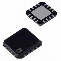
AD8295BCPZ-RL Analog Devices Inc, AD8295BCPZ-RL Datasheet - Page 10

AD8295BCPZ-RL
Manufacturer Part Number
AD8295BCPZ-RL
Description
Dual Precision InAmp
Manufacturer
Analog Devices Inc
Datasheet
1.AD8295ACPZ-R7.pdf
(28 pages)
Specifications of AD8295BCPZ-RL
Amplifier Type
Instrumentation
Number Of Circuits
3
Slew Rate
2 V/µs
Gain Bandwidth Product
1MHz
-3db Bandwidth
1.2MHz
Current - Input Bias
200pA
Voltage - Input Offset
60µV
Current - Supply
2mA
Current - Output / Channel
18mA
Voltage - Supply, Single/dual (±)
4.6 V ~ 36 V, ±2.3 V ~ 18 V
Operating Temperature
-40°C ~ 85°C
Mounting Type
Surface Mount
Package / Case
16-VQFN, CSP Exposed Pad
Lead Free Status / RoHS Status
Lead free / RoHS Compliant
Output Type
-
Lead Free Status / RoHS Status
Lead free / RoHS Compliant
Other names
AD8295BCPZ-RL
AD8295BCPZ-RLTR
AD8295BCPZ-RLTR
AD8295
Figure 10. Input Common-Mode Voltage Range vs. Output Voltage,
Figure 9. Input Common-Mode Voltage Range vs. Output Voltage,
–0.050
–0.100
–0.150
–0.200
–0.250
–0.300
–0.350
–10
–15
–1
–2
–3
–4
15
10
–5
5
4
3
2
1
0
5
0
Figure 11. Input Bias Current vs. Common-Mode Voltage
–15
–5
0
–15
–4
–10
G = 100, V
–10
–3
G = 100, V
–2
COMMON-MODE VOLTAGE (V)
–5
OUTPUT VOLTAGE (V)
OUTPUT VOLTAGE (V)
S
–5
= ±2.5 V, ±5 V, V
–1
S
= ±15 V, V
0
0
0
±5V
REF
1
= 0 V
REF
5
5
= 0 V
2
±15V
G = 100
V
S
= ±2.5V, ±5V
3
10
G = 100
V
S
10
= ±15V
4
15
5
15
Rev. A | Page 10 of 28
Figure 13. Input Bias Current and Input Offset Current vs. Temperature
180
160
140
120
100
Figure 12. Change in Input Offset Voltage vs. Warm-Up Time
2.0
1.8
1.6
1.4
1.2
1.0
0.8
0.6
0.4
0.2
80
60
40
20
–1
–2
–3
–4
–5
5
4
3
2
1
0
0
–40
Figure 14. Positive PSRR vs. Frequency, RTI, G = 1 to 1000
0.1
0
GAIN = 1000
GAIN = 100
GAIN = 10
GAIN = 1
NEGATIVE BIAS CURRENT
–20
1
OFFSET CURRENT
2
0
10
POSITIVE BIAS CURRENT
20
WARM-UP TIME (Min)
TEMPERATURE(°C)
FREQUENCY (Hz)
4
100
40
60
1k
6
80
10k
100
8
100k
120
140
1M
10


