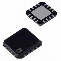
AD8295BCPZ-RL Analog Devices Inc, AD8295BCPZ-RL Datasheet - Page 20

AD8295BCPZ-RL
Manufacturer Part Number
AD8295BCPZ-RL
Description
Dual Precision InAmp
Manufacturer
Analog Devices Inc
Datasheet
1.AD8295ACPZ-R7.pdf
(28 pages)
Specifications of AD8295BCPZ-RL
Amplifier Type
Instrumentation
Number Of Circuits
3
Slew Rate
2 V/µs
Gain Bandwidth Product
1MHz
-3db Bandwidth
1.2MHz
Current - Input Bias
200pA
Voltage - Input Offset
60µV
Current - Supply
2mA
Current - Output / Channel
18mA
Voltage - Supply, Single/dual (±)
4.6 V ~ 36 V, ±2.3 V ~ 18 V
Operating Temperature
-40°C ~ 85°C
Mounting Type
Surface Mount
Package / Case
16-VQFN, CSP Exposed Pad
Lead Free Status / RoHS Status
Lead free / RoHS Compliant
Output Type
-
Lead Free Status / RoHS Status
Lead free / RoHS Compliant
Other names
AD8295BCPZ-RL
AD8295BCPZ-RLTR
AD8295BCPZ-RLTR
AD8295
Reference Terminal
The output voltage of the AD8295 instrumentation amplifier
is developed with respect to the potential on the reference
terminal (REF). This is useful when the output signal needs
to be offset to a precise dc level.
The reference pin input can be driven slightly beyond the rails.
The REF pin is protected with ESD diodes, and the REF voltage
should not exceed either +V
For best performance, the source impedance to the REF terminal
should be kept below 1 Ω. Additional impedance at the REF
terminal can significantly degrade the CMRR of the amplifier.
When the reference source has significant output impedance
(for example, a resistive voltage divider), buffer the signal before
driving the REF pin. Internal Op Amp A1 or A2 can be used for
this purpose, as shown in Figure 60.
R
R
Noise at the reference feeds directly to the output. Therefore, in
Figure 60, Capacitor C is added to filter out any high frequency
noise on the positive power supply line. For very clean supplies,
the capacitor may not be needed. The filter frequency is a trade-
off between noise rejection and start-up time, and is given by
the following equation:
LAYOUT
The AD8295 is a high precision device. To ensure optimum
performance at the PCB level, care must be taken in the board
layout. The AD8295 pins are arranged in a logical manner to
aid in this task.
Routing and Vias
Unlike most LFCSP packages, the AD8295 package was designed
without the thermal pad to allow routes and vias directly beneath
the chip. However, the manufacturing process leaves a very small
section of exposed metal at each of the package corners. This metal
is connected to –V
of a short, vias should not be placed under this exposed metal.
A
B
+V
S
f
LOW
INCORRECT
−
AD8295
PASS
=
REF
Figure 60. Driving the Reference Pin
2
S
π
through the part. Because of the possibility
C
R
1
R
A
A
+
R
S
R
B
or −V
C
B
+
+V
S
S
by more than 0.3 V.
R
R
A
B
AD8295
CORRECT
REF
OP AMP
BUFFER
Rev. A | Page 20 of 28
Careful board layout maximizes system performance. Traces
from the gain setting resistor to the R
short as possible to minimize parasitic inductance. To ensure
the most accurate output, the trace from the REF pin should
either be connected to the local ground of the AD8295 or to a
voltage that is referenced to the local ground of the AD8295.
Common-Mode Rejection over Frequency
The AD8295 has a higher CMRR over frequency than typical
in-amps, which gives it greater immunity to disturbances such
as line noise and its associated harmonics. The AD8295 pinout
and hidden paddle package were designed so that the board
designer can take full advantage of this performance with a
well-implemented layout.
Poor layout can cause some of the common-mode signal to be
converted to a differential signal before it reaches the in-amp.
Such conversions occur when one input path has a frequency
response that is different from the other. To keep CMRR across
frequency high, the input source impedance and capacitance of
each path should be closely matched. Additional source resistance
in the input path (for example, for input protection) should be
placed close to the in-amp inputs to minimize their interaction
with parasitic capacitance from the PCB traces.
Parasitic capacitance at the gain setting pins can also affect
CMRR over frequency. The traces to the R
kept as short as possible. If the board design has a component
at the gain setting pins (for example, a switch or jumper), the
part should be chosen so that the parasitic capacitance is as
small as possible.
Unused Op Amps
When not in use, the internal op amps should be connected in a
unity-gain configuration, with the noninverting input connected
to a bias point in the input range of the op amp. These connections
ensure that the AD8295 op amp uses minimum power and does
not disturb the internal power supplies of the AD8295. These
connections are shown as dotted lines in several of the applica-
tions figures.
Reference
The output voltage of the instrumentation amplifier section of
the AD8295 is developed with respect to the potential on the
reference terminal (REF); care should be taken to tie the REF
pin to the appropriate local ground (see Figure 61).
G
pins should be kept as
G
resistor should be


