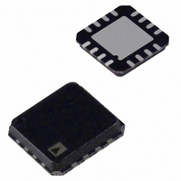
AD8295BCPZ-RL Analog Devices Inc, AD8295BCPZ-RL Datasheet - Page 19

AD8295BCPZ-RL
Manufacturer Part Number
AD8295BCPZ-RL
Description
Dual Precision InAmp
Manufacturer
Analog Devices Inc
Datasheet
1.AD8295ACPZ-R7.pdf
(28 pages)
Specifications of AD8295BCPZ-RL
Amplifier Type
Instrumentation
Number Of Circuits
3
Slew Rate
2 V/µs
Gain Bandwidth Product
1MHz
-3db Bandwidth
1.2MHz
Current - Input Bias
200pA
Voltage - Input Offset
60µV
Current - Supply
2mA
Current - Output / Channel
18mA
Voltage - Supply, Single/dual (±)
4.6 V ~ 36 V, ±2.3 V ~ 18 V
Operating Temperature
-40°C ~ 85°C
Mounting Type
Surface Mount
Package / Case
16-VQFN, CSP Exposed Pad
Lead Free Status / RoHS Status
Lead free / RoHS Compliant
Output Type
-
Lead Free Status / RoHS Status
Lead free / RoHS Compliant
Other names
AD8295BCPZ-RL
AD8295BCPZ-RLTR
AD8295BCPZ-RLTR
THEORY OF OPERATION
As shown in Figure 58, the AD8295 contains a precision
instrumentation amplifier, two uncommitted op amps, and a
precision resistor array. These components allow many common
applications to be wired using simple pin-strapping, directly at
the IC. This not only saves printed circuit board (PCB) space
but also improves circuit performance because both temperature
drift and resistor tolerance errors are reduced.
UNCOMMITTED OP AMPS
The AD8295 has two uncommitted op amps that can be used
independently. These op amps allow simple pin-strapping for
many common applications circuits.
Op Amp A1 has its inverting input connected to a precision 2:1
voltage divider resistor network. Because this network is internal
to the IC, these resistors are closely matched and also track each
other, with temperature variations. Op Amp A1 and the associated
resistor network can be used to create either a noninverting gain
stage of 2 or an inverting gain stage of −1 with excellent gain
accuracy and gain drift.
Op Amp A2 is a more conventional op amp, with standard
inverting and noninverting inputs and an output.
INSTRUMENTATION AMPLIFIER
Gain Selection
The transfer function of the AD8295 is
where placing a resistor across the R
the AD8295 according to the following equation:
V
G 1 +
OUT
=
+IN
–IN
R
R
= G × (V
G
G
49
1
2
3
4
4 .
R
+V
AD8295
–V
16
Figure 58. Functional Block Diagram
G
5
kΩ
S
S
IN+
− V
IA
OUT
REF
15
6
IN−
) + V
A1 OUT
A2 +IN
A1
14
7
REF
A2
G
A2 –IN
terminals sets the gain of
A1 R2
R1
20kΩ
R2
20kΩ
13
8
12
11
10
9
A2 OUT
A1 +IN
A1 R1
A1 –IN
Rev. A | Page 19 of 28
Resistor values can be obtained by referring to Table 9 or by
using the following gain equation:
Table 9. Gains Achieved Using 1% Resistors
1% Standard Table Value of R
49.9 kΩ
12.4 kΩ
5.49 kΩ
2.61 kΩ
1.00 kΩ
499 Ω
249 Ω
100 Ω
49.9 Ω
The AD8295 defaults to G = 1 when no gain resistor is used.
Gain accuracy is a combination of both the R
the accuracy listed in the specifications in Table 2, including
accuracy over temperature. Gain error and gain drift are kept
to a minimum when the gain resistor is not used.
Common-Mode Input Voltage Range
The AD8295 in-amp architecture applies gain internally and
then removes the common-mode voltage. Therefore, internal
nodes in the AD8295 experience a combination of both the
gained signal and the common-mode signal. This combined
signal can be limited by the voltage supplies even when the
individual input and output signals are not. Figure 7 through
Figure 10 show the allowable common-mode input voltage
ranges for various output voltages and supply voltages.
If Figure 7 through Figure 10 indicate that internal voltage
limiting may be an issue, the common-mode range can be
significantly improved by lowering the gain in the instrumen-
tation amplifier by one half and applying a second G = 2 stage.
Figure 59 shows how to do this amplification with the internal
circuitry of the AD8295, requiring no additional external
components.
R
G
Figure 59. Applying Gain in a Later Stage Allows Wider Input
=
+IN
–IN
R
49
G
G
4 .
−
kΩ
IN-AMP
+
–
1
REF
Common-Mode Range
TOTAL GAIN = IN-AMP GAIN × 2
+
–
A1
G
Calculated Gain
1.990
4.984
9.998
19.93
50.40
100
199.4
495
991
R2
20kΩ
R1
20kΩ
G
accuracy and
A1 OUT
AD8295


