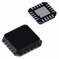
AD8324ACPZ-REEL7 Analog Devices Inc, AD8324ACPZ-REEL7 Datasheet - Page 3

AD8324ACPZ-REEL7
Manufacturer Part Number
AD8324ACPZ-REEL7
Description
IC,TV/VIDEO CIRCUIT,Driver,LLCC,20PIN,PLASTIC
Manufacturer
Analog Devices Inc
Type
Line Driver, Transmitterr
Datasheet
1.AD8324ACPZ.pdf
(16 pages)
Specifications of AD8324ACPZ-REEL7
Applications
Modems, CATV
Mounting Type
Surface Mount
Package / Case
20-LFCSP
Lead Free Status / RoHS Status
Lead free / RoHS Compliant
Available stocks
Company
Part Number
Manufacturer
Quantity
Price
Company:
Part Number:
AD8324ACPZ-REEL7
Manufacturer:
PWRI
Quantity:
2 582
SPECIFICATIONS
T
transformer
Table 1.
Parameter
INPUT CHARACTERISTICS
GAIN CONTROL INTERFACE
OUTPUT CHARACTERISTICS
OVERALL PERFORMANCE
POWER CONTROL
POWER SUPPLY
OPERATING TEMPERATURE RANGE
1
2
3
4
5
6
TOKO 458PT-1556 used for above specifications. Typical insertion loss of 0.5 dB @ 10 MHz.
Guaranteed by design and characterization to ±6 sigma for T
Guaranteed by design and characterization to ±3 sigma for T
Measured through a 1:1 transformer.
Specification is worst case over all gain codes.
V
A
IN
Specified AC Voltage
Input Resistance
Input Capacitance
Voltage Gain Range
Output Step Size
Output Step Size Temperature Coefficient
Bandwidth (–3 dB)
Bandwidth Roll-Off
1 dB Compression Point
Output Noise
Noise Figure
Differential Output Impedance
Second-Order Harmonic Distortion
Third-Order Harmonic Distortion
ACPR
Isolation (Transmit Disable)
TX Enable Settling Time
TX Disable Settling Time
Output Switching Transients
Output Settling
Operating Range
Quiescent Current
= 25°C, V
= 27.5 dBmV, QPSK modulation, 160 kSPS symbol rate.
Max Gain
Min Gain
Max Gain
Min Gain
Transmit Disable
Max Gain
Due to Gain Change
Due to Input Step Change
2, 6
1
CC
2
at the device output.
2
= 3.3 V, R
2
3
L
2
= R
3
IN
5 , 3
= 75 Ω, V
5, 3
IN
(Differential) = 27.5 dBmV, unless otherwise noted. The AD8324 is characterized using a 1:1
A
A
Conditions
Output = 61 dBmV, Max Gain
Single-Ended Input
Differential Input
Gain Code = 60 Dec
Gain Code = 1 Dec
T
All Gain Codes (1–60 Decimal Codes)
f = 65 MHz
Max Gain, f = 10 MHz, Output Referred
Min Gain, f = 10 MHz, Input Referred
f = 10 MHz
f = 10 MHz
f = 10 MHz
f = 10 MHz
TX Enable and TX Disable
f = 33 MHz, V
f = 65 MHz, V
f = 21 MHz, V
f = 65 MHz, V
Max Gain, f = 65 MHz
Max Gain, V
Max Gain, V
Equivalent Output = 31 dBmV
Equivalent Output = 61 dBmV
Min to Max Gain
Max Gain, V
Max Gain
Min Gain
Transmit Disable (TXEN = 0)
SLEEP Mode (Power-Down)
LFCSP
QSOP
= 25°C.
= 25°C.
A
= –40°C to +85°C
Rev. A | Page 3 of 16
IN
IN
IN
OUT
OUT
OUT
OUT
= 0
= 0
= 27.5 dBmV
= 61 dBmV @ Max Gain
= 61 dBmV @ Max Gain
= 61 dBmV @ Max Gain
= 61 dBmV @ Max Gain
Min
58
32.5
–26.5
0.6
19.6
2.1
3.13
195
25
1
–40
–25
Typ
27.5
550
1100
2
59.0
33.5
–25.5
1.0
±0.004
100
1.7
21
3.7
157
1.3
1.1
15.5
75 ± 30%
–66
–58
–59
–54
–61
–75
2.5
3.8
2.5
27
60
30
3.3
207
39
2.5
30
4
Max
60
34.5
–24.5
1.4
166
1.5
1.2
16.0
–60
–53
–57.5
–52.5
–58
–70
6
71
3.47
235
50
4
500
+85
+70
AD8324
Unit
dBmV
Ω
Ω
pF
dB
dB
dB
dB/LSB
dB/°C
MHz
dB
dBm
dBm
nV/√Hz
nV/√Hz
nV/√Hz
dB
Ω
dBc
dBc
dBc
dBc
dBc
dB
μs
μs
mV p-p
mV p-p
ns
ns
V
mA
mA
mA
μA
°C
°C


