AD8324ACP Analog Devices Inc, AD8324ACP Datasheet
AD8324ACP
Specifications of AD8324ACP
Available stocks


Related parts for AD8324ACP


AD8324ACP Summary of contents
Page 1
FEATURES Supports DOCSIS 2.0 and Euro-DOCSIS standards for reverse path transmission systems Gain programmable steps over range Low distortion at 61 dBmV output: –59 dBc SFDR at 21 MHz –54 dBc SFDR at 65 ...
Page 2
AD8324 TABLE OF CONTENTS Specifications..................................................................................... 3 Logic Inputs (TTL/CMOS Compatible Logic)......................... 4 Timing Requirements .................................................................. 4 Absolute Maximum Ratings............................................................ 5 Thermal Resistance ...................................................................... 5 ESD Caution.................................................................................. 5 Pin Configurations and Functional Descriptions ........................ 6 Typical Performance Characteristics ............................................. 7 Applications..................................................................................... ...
Page 3
SPECIFICATIONS T = 25° 3 Ω transformer at the device output. Table 1. Parameter INPUT CHARACTERISTICS Specified AC Voltage Input Resistance Input Capacitance GAIN CONTROL INTERFACE ...
Page 4
AD8324 LOGIC INPUTS (TTL/CMOS COMPATIBLE LOGIC) DATEN , CLK, SDATA, TXEN, SLEEP , V Table 2. Parameter Logic 1 Voltage Logic 0 Voltage = 3.3 V), CLK, SDATA, DATEN Logic 1 Current (V INH = 0 V), CLK, SDATA, DATEN ...
Page 5
... Table 5. Thermal Resistance Ratings –25°C to +70°C Model –65°C to +150°C AD8324JRQ 300°C AD8324ACP 1 Thermal resistance measured on SEMI standard 4-layer board. 2 Thermal resistance measured on SEMI standard 4-layer board, paddle soldered to board. Rev Page AD8324 θ ...
Page 6
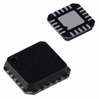
AD8324 PIN CONFIGURATIONS AND FUNCTIONAL DESCRIPTIONS GND 2 GND AD8324 3 V TOP VIEW IN+ (Not to Scale IN– 5 GND Figure 5. 20-Lead LFCSP Table 6. Pin Function Descriptions Pin ...
Page 7
TYPICAL PERFORMANCE CHARACTERISTICS –40 – 62dBmV @ DEC 60 OUT V = 61dBmV @ DEC 60 OUT –60 – 60dBmV @ DEC 60 OUT – FREQUENCY (MHz) Figure 7. Second-Order Harmonic Distortion ...
Page 8
AD8324 0 –10 –20 –30 –40 –50 –60 –70 – –90 CL1 CL1 –100 CENTER 21 MHz 100 kHz/DIV Figure 13. Adjacent Channel Power 40 30 DEC60 20 DEC54 DEC48 10 DEC42 DEC36 0 DEC30 –10 DEC24 DEC18 ...
Page 9
TXEN = 1 140 120 100 GAIN CONTROL (Decimal Code) Figure 19. Output Referred Voltage Noise vs. Gain Control 210 T = ...
Page 10
AD8324 APPLICATIONS GENERAL APPLICATIONS The AD8324 is primarily intended for use as the upstream power amplifier (PA) in DOCSIS (data over cable service interface specification) certified cable modems and CATV set- top boxes. The upstream signal is either a QPSK ...
Page 11
V CC 0.1μ 150Ω 174Ω IN– 0.1μF 1kΩ DATEN 1kΩ SDATA 1kΩ CLK 1kΩ TXEN 1kΩ SLEEP Table 7. Adjacent Channel Power Channel Symbol Rate (kSym/s) 160 320 640 1280 2560 5120 POWER SUPPLY ...
Page 12
AD8324 The BYP pin is used to decouple the output stage to ground. Typically, for normal DOCSIS operation, the BYP pin should be decoupled to ground with a 0.1 μF capacitor. However, in applications that may require transient on/off times ...
Page 13
EVALUATION BOARD FEATURES AND OPERATION The AD8324 evaluation board and control software can be used to control the AD8324 upstream cable driver via the parallel port of a personal computer. A standard printer cable connected to the parallel port of ...
Page 14
AD8324 OVERSHOOT ON PC PRINTER PORTS The data lines on some PC parallel printer ports have excessive overshoot, which may cause communications problems when presented to the CLK pin of the AD8324. The evaluation board was designed to accommodate a ...
Page 15
C1A R2A VIN+_A 0.1μF OPEN T1A 3 1 R1A OPEN R4A 2 73.4Ω VIN–_A TOKO1 R3A C2A R17A OPEN 0.1μF OPEN TP1A R5A R6A 1kΩ 0Ω C3A OPEN TP2A R7A R8A 1kΩ 0Ω C4A ...
Page 16
... AD8324ACP-REEL7 –40°C to +85°C 1 AD8324ACPZ –40°C to +85°C 1 AD8324ACPZ-REEL7 –40°C to +85°C AD8324JRQ-EVAL AD8324ACP-EVAL Pb-free part. © 2005 Analog Devices, Inc. All rights reserved. Trademarks and registered trademarks are the property of their respective owners. 4.00 BSC SQ 0.60 MAX TOP 3 ...