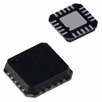
AD8324ACPZ-REEL7 Analog Devices Inc, AD8324ACPZ-REEL7 Datasheet - Page 6

AD8324ACPZ-REEL7
Manufacturer Part Number
AD8324ACPZ-REEL7
Description
IC,TV/VIDEO CIRCUIT,Driver,LLCC,20PIN,PLASTIC
Manufacturer
Analog Devices Inc
Type
Line Driver, Transmitterr
Datasheet
1.AD8324ACPZ.pdf
(16 pages)
Specifications of AD8324ACPZ-REEL7
Applications
Modems, CATV
Mounting Type
Surface Mount
Package / Case
20-LFCSP
Lead Free Status / RoHS Status
Lead free / RoHS Compliant
Available stocks
Company
Part Number
Manufacturer
Quantity
Price
Company:
Part Number:
AD8324ACPZ-REEL7
Manufacturer:
PWRI
Quantity:
2 582
AD8324
PIN CONFIGURATIONS AND FUNCTIONAL DESCRIPTIONS
Table 6. Pin Function Descriptions
Pin No.
20-Lead
LFCSP
1, 2, 5, 9,
18, 19
17, 20
3
4
6
7
8
10
12
13
14
15
16
Pin No.
20-Lead
QSOP
1, 3, 4, 7,
11, 20
2, 19
5
6
8
9
10
12
14
15
16
17
18
GND
GND
GND
V
V
IN+
IN–
Mnemonic
GND
V
V
V
DATEN
SDATA
CLK
SLEEP
BYP
V
V
RAMP
TXEN
CC
IN+
IN–
OUT–
OUT+
1
2
3
4
5
Figure 5. 20-Lead LFCSP
20 19 18
6
(Not to Scale)
TOP VIEW
AD8324
7
8
17
9
Logic 0 disables forward transmission. Logic 1 enables forward transmission.
Description
Common External Ground Reference.
Common Positive External Supply Voltage.
Noninverting Input. DC-biased to approximately V
capacitor.
Inverting Input. DC-biased to approximately V
Data Enable Low Input. This port controls the 8-bit parallel data latch and shift register. A
Logic 0-to-1 transition transfers the latched data to the attenuator core (updates the gain) and
simultaneously inhibits serial data transfer into the register. A 1-to-0 transition inhibits the data
latch (holds the previous and simultaneously enables the register for serial data load).
Serial Data Input. This digital input allows an 8-bit serial (gain) word to be loaded into the internal
register with the MSB (most significant bit) first.
Clock Input. The clock port controls the serial attenuator data transfer rate to the 8-bit master-
slave shift register. Logic 0-to-1 transition latches the data bit, and a 1-to-0 transfers the data bit
to the slave. This requires the input serial data-word to be valid at or before this clock transition.
Low Power Sleep Mode. In the sleep mode, the AD8324’s supply current is reduced to 30 μA. A
Logic 0 powers down the part (high Z
Internal Bypass. This pin must be externally decoupled (0.1 μF capacitor).
Negative Output Signal. Must be biased to V
Positive Output Signal. Must be biased to V
External RAMP Capacitor (Optional).
16
10
15
14
13
12
11
RAMP
V
V
BYP
NC
OUT+
OUT–
Rev. A | Page 6 of 16
OUT
state), and a Logic 1 powers up the part.
CC
CC
. See Figure 23.
. See Figure 23.
CC
/2. Should be ac-coupled with a 0.1 μF capacitor.
CC
/2. Should be ac-coupled with a 0.1 μF
DATEN
SDATA
GND
GND
GND
GND
CLK
V
V
V
IN+
CC
IN–
Figure 6. 20-Lead QSOP
10
NC = NO CONNECT
1
2
3
4
5
6
7
8
9
(Not to Scale)
AD8324
TOP VIEW
20
19
18
17
16
15
14
13
12
11
TXEN
RAMP
BYP
NC
V
V
V
SLEEP
GND
GND
CC
OUT+
OUT–


