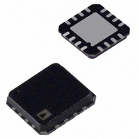
AD8396ACPZ-RL Analog Devices Inc, AD8396ACPZ-RL Datasheet

AD8396ACPZ-RL
Specifications of AD8396ACPZ-RL
Related parts for AD8396ACPZ-RL
AD8396ACPZ-RL Summary of contents
Page 1
FEATURES 2 differential DSL channels comprised of current feedback, high output current amplifiers Integrated feedback and gain resistors Integrated biasing network Ideal for use as ADSL/ADSL2+ dual-channel Central Office (CO) line drivers Low power consumption Dual-supply operation from ±6 V ...
Page 2
AD8396 TABLE OF CONTENTS Features .............................................................................................. 1 Applications ....................................................................................... 1 General Description ......................................................................... 1 Pin Configuration ............................................................................. 1 Revision History ............................................................................... 2 Specifications ..................................................................................... 3 Absolute Maximum Ratings ............................................................ 4 Thermal Resistance ...................................................................... 4 Maximum Power Dissipation ..................................................... 4 ESD ...
Page 3
SPECIFICATIONS (V − 100 Ω (fixed (0 25°C, typical DSL application circuit, unless otherwise noted DIFF Table 1. Parameter DYNAMIC PERFORMANCE −3 dB ...
Page 4
AD8396 ABSOLUTE MAXIMUM RATINGS Table 2. Parameter Supply Voltage, V − Power Dissipation Storage Temperature Range Operating Temperature Range Lead Temperature (Soldering, 10 sec) Junction Temperature Stresses above those listed under Absolute Maximum Ratings may cause permanent ...
Page 5
PIN CONFIGURATION AND FUNCTION DESCRIPTIONS Table 4. Pin Function Descriptions Pin No. Mnemonic 1 INPA 2 INNA 3, 11 DGND 4 INPB 5 INNB 6 VCOM-B 7 PD_B 8 VEE 9 VONB 10 VOPB 12 VONA 13 VOPA 14 VCC ...
Page 6
AD8396 TYPICAL PERFORMANCE CHARACTERISTICS –1 –2 –3 –4 –5 2V p-p –6 –7 –8 0 0.1 1 FREQUENCY (MHz) Figure 5. Differential Gain vs. Frequency ...
Page 7
V = ±12V ±10V –5 –10 0 0.2 0.4 0.6 0.8 1.0 1.2 1.4 TIME (μs) Figure 11. Output Overdrive Recovery, Typical ADSL/ADSL2+ Application Circuit 3 ...
Page 8
AD8396 THEORY OF OPERATION The AD8396 is a current feedback amplifier with high output current capability. With a current feedback amplifier, the current into the inverting input is the feedback signal, and the open-loop behavior is that of a transimpedance, ...
Page 9
APPLICATIONS INFORMATION SUPPLIES, GROUNDING, AND LAYOUT The AD8396 can be powered from either single or dual supplies, with the total supply voltage ranging from For optimum performance, use well-regulated low ripple supplies. As with all ...
Page 10
AD8396 LIGHTNING AND AC POWER FAULT When the AD8396 is an ADSL/ADSL2+ line driver transformer coupled to the twisted pair telephone line. In this environment, the AD8396 is subject to large line transients, resulting from events, such as ...
Page 11
... OUTLINE DIMENSIONS PIN 1 INDICATOR 0.80 0.75 0.70 SEATING PLANE ORDERING GUIDE Model Temperature Range 1 AD8396ACPZ-R2 −40°C to +85°C 1 AD8396ACPZ-RL −40°C to +85°C 1 AD8396ACPZ-R7 −40°C to +85° RoHS Compliant Part. 4.10 0.35 4.00 SQ 0.30 3.90 0.25 13 0.65 12 BSC EXPOSED ...
Page 12
AD8396 NOTES ©2007–2009 Analog Devices, Inc. All rights reserved. Trademarks and registered trademarks are the property of their respective owners. D07022-0-8/09(C) Rev Page ...


