AD9212-65EBZ Analog Devices Inc, AD9212-65EBZ Datasheet
AD9212-65EBZ
Specifications of AD9212-65EBZ


Related parts for AD9212-65EBZ


AD9212-65EBZ Summary of contents
Page 1
... Tape drives Optical networking Test equipment GENERAL DESCRIPTION The AD9212 is an octal, 10-bit, 40 MSPS/65 MSPS ADC with an on-chip sample-and-hold circuit designed for low cost, low power, small size, and ease of use. Operating at a conversion rate MSPS optimized for outstanding dynamic performance and low power in applications where a small package size is critical ...
Page 2
... AD9212 TABLE OF CONTENTS Features .............................................................................................. 1 Applications ....................................................................................... 1 General Description ......................................................................... 1 Functional Block Diagram .............................................................. 1 Product Highlights ........................................................................... 1 Revision History ............................................................................... 2 Specifications ..................................................................................... 3 AC Specifications .......................................................................... 4 Digital Specifications ................................................................... 5 Switching Specifications .............................................................. 6 Timing Diagrams .......................................................................... 7 Absolute Maximum Ratings ............................................................ 9 Thermal Impedance ..................................................................... 9 ESD Caution .................................................................................. 9 Pin Configuration and Function Descriptions ........................... 10 Equivalent Circuits ......................................................................... 12 Typical Performance Characteristics ........................................... 14 Theory of Operation ...................................................................... 19 Analog Input Considerations ...
Page 3
... Full 1.7 1.8 1.9 Full 252 260 Full 49.5 53 Full 542 560 Full 3 11 Full 83 Full −90 Full −90 Rev Page AD9212 AD9212-65 Min Typ Max Unit 10 Bits Guaranteed ±1.5 ±8 mV ±3 ±8 mV ±3.2 ±4 ±0.4 ±0 ±0.3 ±0.65 LSB ±0.4 ± ...
Page 4
... Full 74 Full −87 Full −85 Full −79 25°C Full −74 Full −90 Full −85 Full −85 Full −85 25°C 80.0 25°C 77.0 Rev Page AD9212-65 Max Min Typ Max Unit 60.8 dB 60.8 dB 58.5 60.8 dB 60.7 dB 60.7 dB 60.6 dB 57.0 60.5 dB 60.4 dB 9.81 Bits 9 ...
Page 5
... Full 1.79 Full 0.05 LVDS Full 247 454 Full 1.125 1.375 Offset binary LVDS Full 150 250 Full 1.10 1.30 Offset binary Rev Page AD9212 AD9212-65 Min Typ Max Unit CMOS/LVDS/LVPECL 250 mV p-p 1 kΩ 1.5 pF 1.2 3 kΩ 0 ...
Page 6
... SAMPLE SAMPLE SAMPLE (t /20) − 300 (t /20) (t /20) + 300 SAMPLE SAMPLE SAMPLE ±50 ±200 600 375 8 750 <1 1 Rev Page AD9212-65 Min Typ Max 65 10 7.7 7.7 1.5 2.3 3.1 300 300 1.5 2.3 3 FCO (t /20) SAMPLE (t /20) − 300 ...
Page 7
... Figure 2. 10-Bit Data Serial Stream (Default), MSB First FRAME t DATA MSB D10 – – – – – – 9 Figure 3.12-Bit Data Serial Stream, MSB First Rev Page MSB – – – – – – – MSB N – – – – – – – 8 AD9212 – 8 D10 N – 8 ...
Page 8
... AD9212 N – 1 VIN ± CLK– CLK+ t CPD DCO– DCO+ t FCO FCO– FCO – FRAME t DATA LSB – – – – – – – 9 Figure 4. 10-Bit Data Serial Stream, LSB First Rev Page LSB – – – – – – ...
Page 9
... PCB. −0 +2.0 V ESD CAUTION −0 +3.9 V −0 +2.0 V −0 +2.0 V −0 +3.9 V −0 +2.0 V −0 +2.0 V −40°C to +85°C −65°C to +150°C 150°C 300°C Rev Page AD9212 1 θ θ θ Unit 17.7 °C/W 15.5 8.7 0.6 ° ...
Page 10
... D − − − B PIN 1 INDICATOR AVDD AVDD 4 EXPOSED PADDLE, PIN 0 5 (BOTTOM OF PACKAGE) 6 AVDD 7 AD9212 AVDD 8 TOP VIEW CLK– 9 (Not to Scale) CLK+ 10 AVDD 11 AVDD – Figure 5. 64-Lead LFCSP Pin Configuration, Top View Description Analog Ground (Exposed Paddle) 1.8 V Analog Supply Digital Output Driver Ground 1 ...
Page 11
... ADC D Analog Input True External Resistor to Set the Internal ADC Core Bias Current Reference Mode Selection Voltage Reference Input/Output Negative Differential Reference Positive Differential Reference ADC E Analog Input True ADC E Analog Input Complement ADC F Analog Input Complement ADC F Analog Input True Rev Page AD9212 ...
Page 12
... AD9212 EQUIVALENT CIRCUITS VIN ± x Figure 6. Equivalent Analog Input Circuit 10Ω CLK+ 10kΩ 10kΩ 10Ω CLK– Figure 7. Equivalent Clock Input Circuit 350Ω SDIO/ODM 30kΩ Figure 8. Equivalent SDIO/ODM Input Circuit 1.25V SCLK/DTP OR PDWN Rev Page DRVDD – x ...
Page 13
... AVDD 70kΩ 1kΩ CSB Figure 12. Equivalent CSB Input Circuit 1kΩ SENSE Figure 13. Equivalent SENSE Circuit VREF Figure 14. Equivalent VREF Circuit Rev Page AD9212 6kΩ ...
Page 14
... Figure 20. Single-Tone 32k FFT with f Rev Page AIN = –0.5dBFS SNR = 60.41dB ENOB = 9.7 SFDR = 76.11dBc FREQUENCY (MHz MHz, AD9212- AIN = –0.5dBFS SNR = 60.25dB ENOB = 9.66 SFDR = 72.45dBc FREQUENCY (MHz MHz, AD9212- AIN = –0.5dBFS SNR = 60.08dB ENOB = 9.61 SFDR = 71.68dBc FREQUENCY (MHz) = 120 MHz, AD9212- ...
Page 15
... Figure 26. SNR/SFDR vs. Analog Input Level, f Rev Page AD9212 SFDR SNR ENCODE RATE (MSPS MHz, AD9212-65 SAMPLE IN SFDR 70dB REFERENCE SNR –50 –40 –30 –20 –10 ANALOG INPUT LEVEL (dBFS) = 10.3 MHz, AD9212-40 IN SFDR 70dB REFERENCE SNR –50 –40 –30 –20 – ...
Page 16
... Figure 31. Two-Tone 32k FFT with MHz and IN1 MHz, AD9212-65 IN2 0 AIN1 AND AIN2 = –7dBFS SFDR = 72.5dB IMD2 = 77.14dBc IMD3 = 72.55dBc –20 –40 –60 – FREQUENCY (MHz) Figure 32. Two-Tone 32k FFT with MHz and IN1 MHz, AD9212- 65 IN2 MHz, IN2 30 30 ...
Page 17
... Rev Page AD9212 200 400 600 800 CODE Figure 36. INL 2.3 MHz, AD9212-65 IN 200 400 600 800 CODE Figure 37. DNL 2.3 MHz, AD9212- FREQUENCY (MHz) Figure 38. CMRR vs. Frequency, AD9212-65 1000 1000 40 ...
Page 18
... Figure 40. Noise Power Ratio (NPR), AD9212 0.096 LSB rms –1 –2 –3 –4 –5 –6 –7 –8 –9 –10 – Figure 41. Full Power Bandwidth vs. Frequency, AD9212- Rev Page –3dB BANDWIDTH = 325MHz 50 100 150 200 250 300 350 400 450 FREQUENCY (MHz) 500 ...
Page 19
... Front-End for Wideband A/D for more information. In general, the precise values depend on the application. The analog inputs of the AD9212 are not internally dc-biased. Therefore, in ac-coupled applications, the user must provide this bias externally. Setting the device so that V recommended for optimum performance, but the device can function over a wider range with reasonable performance, as shown in Figure 45 and Figure 46 ...
Page 20
... Rev Page SFDR SNR 0.6 0.9 1.2 ANALOG INPUT COMMON-MODE VOLTAGE (V) Figure 45. SNR/SFDR vs. Common-Mode Voltage 2.3 MHz, AD9212-65 IN SFDR SNR 0.6 0.9 1.2 ANALOG INPUT COMMON-MODE VOLTAGE (V) Figure 46. SNR/SFDR vs. Common-Mode Voltage MHz, AD9212-65 IN 1.5 1.5 ...
Page 21
... In the case of the AD9212, the largest input span available p-p. Differential Input Configurations There are several ways to drive the AD9212 either actively or passively; however, optimum performance is achieved by driving the analog input differentially. For example, using the ...
Page 22
... This allows a wide range of clock input duty cycles without affecting the performance of the AD9212. When the DCS is on, noise and distortion perfor- mance are nearly flat for a wide range of duty cycles. However, some applications may require the DCS function to be off. If so, 0.1µ ...
Page 23
... Figure 56). The clock input should be treated as an analog signal in cases where aperture jitter may affect the dynamic range of the AD9212. Power supplies for clock drivers should be separated from the ADC output driver supplies to avoid modulating the clock signal with digital noise ...
Page 24
... An example of the FCO and data stream when the AD9212 is used with traces of proper length and position is shown in Figure 59. CH1 500mV/DIV = FCO ...
Page 25
... Digital Output Offset Binary Input Span = 2 V p-p (V) (D9 ... D0) +1.00 11 1111 1111 0.00 10 0000 0000 −0.001953 01 1111 1111 −1.00 00 0000 0000 AD9212 1.5ns 150ps ...
Page 26
... AD9212 Two output clocks are provided to assist in capturing data from the AD9212. The DCO is used to clock the output data and is equal to five times the sample clock (CLK) rate. Data is clocked out of the AD9212 and must be captured on the rising and Table 9. Flexible Output Test Modes ...
Page 27
... Section 5.6 of the ITU-T 0.150 (05/96) standard. The only differences are that the starting value must be a specific value instead of all 1s (see Table 10 for the initial values) and the AD9212 inverts the bit stream with relation to the ITU standard. Table 10. PN Sequence Initial ...
Page 28
... Voltage Reference A stable, accurate 0.5 V voltage reference is built into the AD9212. This is gained up internally by a factor of 2, setting VREF to 1.0 V, which results in a full-scale differential input span p-p. VREF is set internally by default; however, the VREF pin can be driven externally with a 1.0 V reference to improve accuracy ...
Page 29
... REFT and REFB, for the ADC core. Therefore, the external reference must be limited to a nominal voltage of 1.0 V. 0.02 0 –0.02 –0.04 –0.06 –0.08 –0.10 –0.12 –0.14 –0.16 –0.18 –40 –20 0 Figure 66. Typical VREF Drift Rev Page AD9212 TEMPERATURE (°C) ...
Page 30
... If multiple SDIO pins share a common connection, care should be taken to ensure that proper V load for each AD9212, Figure 67 shows the number of SDIO pins that can be connected together and the resulting V This interface is flexible enough to be controlled by either serial ...
Page 31
... Minimum time for the SDIO pin to switch from an input to an output relative to the SCLK falling edge (not shown in Figure 68) Minimum time for the SDIO pin to switch from an output to an input relative to the SCLK rising edge (not shown in Figure 68) Rev Page 100 AD9212 DON’T CARE DON’T CARE ...
Page 32
... Addresses that have values marked as 0 should be considered reserved and have 0 written to their registers during power-up. DEFAULT VALUES When the AD9212 comes out of a reset, critical registers are preloaded with default values. These values are indicated in Table 16, where an X refers to an undefined feature. ...
Page 33
... Bit 5 Bit 4 Bit 3 Bit 2 Soft 1 1 Soft reset reset off 0 = off (default) (default) 10-bit Chip ID Bits [7:0] (AD9212 = 0x08), (default Data Data Channel Channel (default) (default off 0 = off Clock Clock Data Data ...
Page 34
... AD9212 Addr. (MSB) (Hex) Parameter Name Bit 7 Bit 6 14 output_mode LVDS ANSI-644 (default LVDS low power, (IEEE 1596.3 similar) 15 output_adjust output_phase user_patt1_lsb user_patt1_msb B15 B14 1B user_patt2_lsb user_patt2_msb B15 B14 21 serial_control LSB first off (default) 22 serial_ch_stat undefined feature Bit 5 Bit 4 Bit 3 Bit 2 ...
Page 35
... APPLICATIONS INFORMATION DESIGN GUIDELINES Before starting design and layout of the AD9212 as a system recommended that the designer become familiar with these guidelines, which discuss the special circuit connections and layout requirements needed for certain pins. Power and Ground Recommendations When connecting power to the AD9212 recommended that two separate 1 ...
Page 36
... Figure 74 to Figure 78). Figure 70 shows the typical bench characterization setup used to evaluate the ac performance of the AD9212 critical that the signal sources used for the analog input and clock have very low phase noise (<1 ps rms jitter) to realize the optimum performance of the converter ...
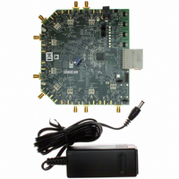
Page 37
... DEFAULT OPERATION AND JUMPER SELECTION SETTINGS The following is a list of the default and optional settings or modes allowed on the AD9212 Rev. A evaluation board. Power: Connect the switching power supply that is provided with the evaluation kit between a rated 100 240 V ac wall outlet and P701. ...
Page 38
... Input Signal = −1.03 dBFS, SNR = 56.75 dBc, SFDR = 64.4 dBc) Rev Page 680nH 68pF 680nH 65MSPS SAMPLE AIN = 3.5MHz –20 AD8334 = MAX GAIN SETTING –40 –60 –80 0 2.5 5.0 7.5 10.0 12.5 15.0 17.5 20.0 22.5 25.0 27.5 30.0 32.5 FREQUENCY (MHz) Figure 73. AD9212 FFT Example Results Using ...
Page 39
... Figure 74. Evaluation Board Schematic, DUT Analog Inputs Rev Page AD9212 05968-072 ...
Page 40
... AD9212 Figure 75. Evaluation Board Schematic, DUT Analog Inputs (Continued) Rev Page 05968-073 ...
Page 41
... CHB 30 CHC D+C 29 D−C CHC 28 D+D CHD 27 D−D CHD 26 FCO FCO+ 25 FCO− FCO 24 DCO DCO+ 23 DCO− DCO 22 D+E CHE 21 CHE D−E 20 D+F CHF 19 D−F CHF 18 D+G CHG 17 D−G CHG Rev Page AD9212 05968-074 AVDD_DUT CW GND ...
Page 42
... AD9212 GND RSET S10 6 VREF Figure 77. Evaluation Board Schematic, Clock Circuitry Rev Page 05968-075 ...
Page 43
... COM3 R508 274Ω C521 0.018µF C520 22pF L503 120nH 0.1µF C519 GND VG34 External Variable Gain Drive AD9212 05968-076 C535 C536 10µF 0.1µF R512 R511 10kΩ 10kΩ R509 274Ω C527 0.018µF C526 22pF ...
Page 44
... AD9212 C610 C609 10µF 0.1µF R605 AVDD_5V 10kΩ AVDD_5V C605 0.1µF R603 274Ω C602 0.018µF 0.1µF C601 AVDD_5V CW GND VG56 Variabl e Gain Circuit (0−1.0V DC) VG56 External Variable Gain Drive Figure 79. Evaluation Board Schematic, Optional DUT Analog Input Drive (Continued) R613 187Ω ...
Page 45
... OPTIONAL GREEN Figure 80. Evaluation Board Schematic, Power Supply Inputs and SPI Interface Circuitry C702 C703 0.1µF 0.1µF PICVCC 1 2 PICVCC GP1 3 4 GP1 GP0 5 6 GP0 MCLR/GP3 8 7 MCLR/GP3 9 10 Rev Page AD9212 05968-078 GND GND 1 1 GND GND ...
Page 46
... AD9212 Figure 81. Evaluation Board Layout, Primary Side Rev Page ...
Page 47
... Figure 82. Evaluation Board Layout, Ground Plane Rev Page AD9212 ...
Page 48
... AD9212 Figure 83. Evaluation Board Layout, Power Plane Rev Page ...
Page 49
... Figure 84. Evaluation Board Layout, Secondary Side (Mirrored Image) Rev Page AD9212 ...
Page 50
... AD9212 Table 17. Evaluation Board Bill of Materials (BOM) Qty per Reference Board Designator Item 1 1 AD9212LFCSP_REVA 2 118 C101, C102, C107, C108, C109, C114, C115, C116, C121, C122, C123, C128, C201, C202, C207, C208, C209, C214, C215, C216, C221, C222, C223, C228, C301, C302, C304, ...
Page 51
... Ferrite bead 1210 10 μH, bead core 3.2 × 2.5 × 1.6 SMD Inductor 402 120 nH, test freq 100 MHz, 5% tol, 150 mA Rev Page AD9212 Manufacturer Manufacturer Part Number Murata GRM1555C1H220JZ01D ROHM Co., Ltd. TCA1C106M8R Murata GRM188R61C105KA93D Murata GRM21BR71H104KA01L ...
Page 52
... AD9212 Qty per Reference Item Board Designator 26 32 L505, L506, L507, L508, L509, L510, L511, L512, L513, L514, L515, L516, L517, L518, L519, L520, L605, L606, L607, L608, L609, L610, L611, L612, L613, L614, L615, L616, L617, L618, L619, L620 27 1 OSC401 ...
Page 53
... W, 1% tol Resistor 603 261 Ω, 1/ tol Resistor 402 240 Ω, 1/ tol Resistor 402 100 Ω, 1/ tol Switch SMD Light Touch, 100 GE Rev Page AD9212 Manufacturer Manufacturer Part Number NIC NRC04F4990TRF Components Corp. NIC NRC04F1003TRF Components Corp. NIC NRC04F4121TRF Components Corp ...
Page 54
... A, 1.8 V LDO regulator IC CP-64-3 AD8334ACPZ-REEL, ultralow noise precision dual VGA IC SOT-223 ADP3339AKC-5-RL7 IC SOT-223 ADP3339AKC-3.3-RL IC CP-64-3 AD9212BCPZ-65, octal, 10-bit, 65 MSPS serial LVDS 1.8 V ADC IC SOT-23 ADR510ARTZ, 1.0 V, precision low noise shunt voltage reference IC LFCSP AD9515BCPZ, 1.6 GHz CP-32-2 clock distribution IC IC ...
Page 55
... PLANE ORDERING GUIDE 1 Model Temperature Range AD9212ABCPZ-40 −40°C to +85°C AD9212ABCPZRL7-40 −40°C to +85°C AD9212ABCPZ-65 −40°C to +85°C AD9212ABCPZRL7-65 −40°C to +85°C AD9212-65EBZ RoHS Compliant Part. 9.00 0.60 MAX 0.60 MAX 49 48 0.50 8.75 BSC BSC SQ 0. ...
Page 56
... AD9212 NOTES ©2006–2010 Analog Devices, Inc. All rights reserved. Trademarks and registered trademarks are the property of their respective owners. D05968-0-5/10(D) Rev Page ...