AD9212-65EBZ Analog Devices Inc, AD9212-65EBZ Datasheet - Page 30
AD9212-65EBZ
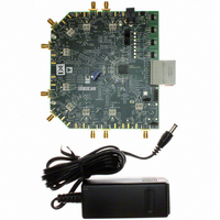
Manufacturer Part Number
AD9212-65EBZ
Description
Octal 10 Bit, 65 MSPS Serial LVDS ADC EB
Manufacturer
Analog Devices Inc
Datasheet
1.AD9212ABCPZRL7-40.pdf
(56 pages)
Specifications of AD9212-65EBZ
Number Of Adc's
8
Number Of Bits
10
Sampling Rate (per Second)
65M
Data Interface
Serial
Inputs Per Adc
1 Differential
Input Range
2 Vpp
Power (typ) @ Conditions
100mW @ 65MSPS
Voltage Supply Source
Analog and Digital
Operating Temperature
-40°C ~ 85°C
Utilized Ic / Part
AD9212
Lead Free Status / RoHS Status
Lead free / RoHS Compliant


AD9212
SERIAL PORT INTERFACE (SPI)
The AD9212 serial port interface allows the user to configure
the converter for specific functions or operations through a
structured register space provided inside the ADC. This may
provide the user with additional flexibility and customization,
depending on the application. Addresses are accessed via the
serial port and can be written to or read from via the port. Memory
is organized into bytes that can be further divided into fields, as
documented in the Memory Map section. Detailed operational
information can be found in the
Interfacing to High Speed ADCs via SPI.
Three pins define the SPI: the SCLK, SDIO, and CSB pins (see
Table 14). The SCLK pin is used to synchronize the read and write
data presented to the ADC. The SDIO pin is a dual-purpose pin
that allows data to be sent to and read from the internal ADC
memory map registers. The CSB pin is an active low control
that enables or disables the read and write cycles.
Table 14. Serial Port Pins
Pin
SCLK
SDIO
CSB
The falling edge of the CSB in conjunction with the rising edge
of the SCLK determines the start of the framing sequence. During
an instruction phase, a 16-bit instruction is transmitted, followed
by one or more data bytes, which is determined by Bit Field W0
and Bit Field W1. An example of the serial timing and its
definitions can be found in Figure 68 and Table 15.
During normal operation, CSB is used to signal to the device
that SPI commands are to be received and processed. When
CSB is brought low, the device processes SCLK and SDIO to
execute instructions. Normally, CSB remains low until the
communication cycle is complete. However, if connected to a
slow device, CSB can be brought high between bytes, allowing
older microcontrollers enough time to transfer data into shift
registers. CSB can be stalled when transferring one, two, or
three bytes of data.
When W0 and W1 are set to 11, the device enters streaming
mode and continues to process data, either reading or writing,
until CSB is taken high to end the communication cycle. This
allows complete memory transfers without requiring additional
instructions.
Function
Serial Clock. The serial shift clock input, which is used to
synchronize serial interface reads and writes.
Serial Data Input/Output. A dual-purpose pin that typically
serves as an input or output, depending on the instruction
sent and the relative position in the timing frame.
Chip Select Bar (Active Low). This control gates the read
and write cycles.
AN-877 Application
Note,
Rev. D | Page 30 of 56
Regardless of the mode, if CSB is taken high in the middle of a
byte transfer, the SPI state machine is reset and the device waits
for a new instruction.
In addition to the operation modes, the SPI port configuration
influences how the AD9212 operates. For applications that do
not require a control port, the CSB line can be tied and held high.
This places the remainder of the SPI pins into their secondary
modes, as defined in the SDIO/ODM Pin and SCLK/DTP Pin
sections. CSB can also be tied low to enable 2-wire mode. When
CSB is tied low, SCLK and SDIO are the only pins required for
communication. Although the device is synchronized during
power-up, the user should ensure that the serial port remains
synchronized with the CSB line when using this mode. When
operating in 2-wire mode, it is recommended that a 1-, 2-, or 3-
byte transfer be used exclusively. Without an active CSB line,
streaming mode can be entered but not exited.
In addition to word length, the instruction phase determines if
the serial frame is a read or write operation, allowing the serial
port to be used to both program the chip and read the contents
of the on-chip memory. If the instruction is a readback operation,
performing a readback causes the SDIO pin to change from an
input to an output at the appropriate point in the serial frame.
Data can be sent in MSB- or LSB-first mode. MSB-first mode
is the default at power-up and can be changed by adjusting the
configuration register. For more information about this and
other features, see the AN-877 Application Note, Interfacing to
High Speed ADCs via SPI.
HARDWARE INTERFACE
The pins described in Table 14 constitute the physical interface
between the user’s programming device and the serial port of
the AD9212. The SCLK and CSB pins function as inputs when
using the SPI. The SDIO pin is bidirectional, functioning as an
input during write phases and as an output during readback.
If multiple SDIO pins share a common connection, care should be
taken to ensure that proper V
load for each AD9212, Figure 67 shows the number of SDIO pins
that can be connected together and the resulting V
This interface is flexible enough to be controlled by either serial
PROMs or PIC mirocontrollers, providing the user with an
alternative method, other than a full SPI controller, to program
the ADC (see the
If the user chooses not to use the SPI, these dual-function pins
serve their secondary functions when the CSB is strapped to
AVDD during device power-up. See the Theory of Operation
section for details on which pin-strappable functions are
supported on the SPI pins.
AN-812 Application
OH
levels are met. Assuming the same
Note).
OH
level.
Related parts for AD9212-65EBZ
Image
Part Number
Description
Manufacturer
Datasheet
Request
R

Part Number:
Description:
±1.7g Dual-Axis IMEMS Accelerometer Evaluation Board
Manufacturer:
Analog Devices Inc
Datasheet:

Part Number:
Description:
Inertial Sensor Evaluation System
Manufacturer:
Analog Devices Inc
Datasheet:
Part Number:
Description:
Manufacturer:
Analog Devices Inc
Datasheet:
Part Number:
Description:
Manufacturer:
Analog Devices Inc
Datasheet:
Part Number:
Description:
Manufacturer:
Analog Devices Inc
Datasheet:
Part Number:
Description:
Manufacturer:
Analog Devices Inc
Datasheet:
Part Number:
Description:
Manufacturer:
Analog Devices Inc
Datasheet:
Part Number:
Description:
Manufacturer:
Analog Devices Inc
Datasheet:
Part Number:
Description:
Manufacturer:
Analog Devices Inc
Datasheet:
Part Number:
Description:
Manufacturer:
Analog Devices Inc
Datasheet:
Part Number:
Description:
Manufacturer:
Analog Devices Inc
Datasheet:
Part Number:
Description:
Manufacturer:
Analog Devices Inc
Datasheet:
Part Number:
Description:
Manufacturer:
Analog Devices Inc
Datasheet: