AD9212-65EBZ Analog Devices Inc, AD9212-65EBZ Datasheet - Page 32
AD9212-65EBZ
Manufacturer Part Number
AD9212-65EBZ
Description
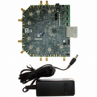
Octal 10 Bit, 65 MSPS Serial LVDS ADC EB
Manufacturer
Analog Devices Inc
Datasheet
1.AD9212ABCPZRL7-40.pdf
(56 pages)
Specifications of AD9212-65EBZ
Number Of Adc's
8
Number Of Bits
10
Sampling Rate (per Second)
65M
Data Interface
Serial
Inputs Per Adc
1 Differential
Input Range
2 Vpp
Power (typ) @ Conditions
100mW @ 65MSPS
Voltage Supply Source
Analog and Digital
Operating Temperature
-40°C ~ 85°C
Utilized Ic / Part
AD9212
Lead Free Status / RoHS Status
Lead free / RoHS Compliant


AD9212
MEMORY MAP
READING THE MEMORY MAP TABLE
Each row in the memory map register table (Table 16) has eight
address locations. The memory map is divided into three sections:
the chip configuration register map (Address 0x00 to Address 0x02),
the device index and transfer register map (Address 0x04,
Address 0x05, and Address 0xFF), and the ADC functions register
map (Address 0x08 to Address 0x22).
The leftmost column of the memory map indicates the register
address number; the default value is shown in the second right-
most column. The Bit 7 column is the start of the default
hexadecimal value given. For example, Address 0x09, the clock
register, has a default value of 0x01, meaning Bit 7 = 0, Bit 6 = 0,
Bit 5 = 0, Bit 4 = 0, Bit 3 = 0, Bit 2 = 0, Bit 1 = 0, and Bit 0 = 1, or
0000 0001 in binary. This setting is the default for the duty cycle
stabilizer in the on condition. By writing 0 to Bit 0 of this address
followed by writing 0x01 in Register 0xFF (transfer bit), the duty
cycle stabilizer turns off. It is important to follow each writing
sequence with a transfer bit to update the SPI registers. All
registers, except Register 0x00, Register 0x04, Register 0x05, and
Register 0xFF, are buffered with a master-slave latch and require
writing to the transfer bit. For more information on this and
other functions, consult the
Interfacing to High Speed ADCs via SPI.
AN-877 Application
Note,
Rev. D | Page 32 of 56
RESERVED LOCATIONS
Undefined memory locations should not be written to except
when writing the default values suggested in this data sheet.
Addresses that have values marked as 0 should be considered
reserved and have 0 written to their registers during power-up.
DEFAULT VALUES
When the AD9212 comes out of a reset, critical registers are
preloaded with default values. These values are indicated in
Table 16, where an X refers to an undefined feature.
LOGIC LEVELS
An explanation of various registers follows: “bit is set” is
synonymous with “bit is set to Logic 1” or “writing Logic 1 for
the bit. ” Similarly, “clear a bit” is synonymous with “bit is set to
Logic 0” or “writing Logic 0 for the bit. ”
Related parts for AD9212-65EBZ
Image
Part Number
Description
Manufacturer
Datasheet
Request
R

Part Number:
Description:
±1.7g Dual-Axis IMEMS Accelerometer Evaluation Board
Manufacturer:
Analog Devices Inc
Datasheet:

Part Number:
Description:
Inertial Sensor Evaluation System
Manufacturer:
Analog Devices Inc
Datasheet:
Part Number:
Description:
Manufacturer:
Analog Devices Inc
Datasheet:
Part Number:
Description:
Manufacturer:
Analog Devices Inc
Datasheet:
Part Number:
Description:
Manufacturer:
Analog Devices Inc
Datasheet:
Part Number:
Description:
Manufacturer:
Analog Devices Inc
Datasheet:
Part Number:
Description:
Manufacturer:
Analog Devices Inc
Datasheet:
Part Number:
Description:
Manufacturer:
Analog Devices Inc
Datasheet:
Part Number:
Description:
Manufacturer:
Analog Devices Inc
Datasheet:
Part Number:
Description:
Manufacturer:
Analog Devices Inc
Datasheet:
Part Number:
Description:
Manufacturer:
Analog Devices Inc
Datasheet:
Part Number:
Description:
Manufacturer:
Analog Devices Inc
Datasheet:
Part Number:
Description:
Manufacturer:
Analog Devices Inc
Datasheet: