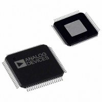
AD9410BSVZ Analog Devices Inc, AD9410BSVZ Datasheet

AD9410BSVZ
Specifications of AD9410BSVZ
Available stocks
Related parts for AD9410BSVZ
AD9410BSVZ Summary of contents
Page 1
FEATURES SNR = 54 dB with 99 MHz analog input 500 MHz analog bandwidth On-chip reference and track and hold 1.5 V p-p differential analog input range 5.0 V and 3.3 V supply operation 3.3 V CMOS/TTL outputs Power: 2.1 ...
Page 2
AD9410 TABLE OF CONTENTS Features .............................................................................................. 1 Applications....................................................................................... 1 Functional Block Diagram .............................................................. 1 General Description ......................................................................... 1 Product Highlights ........................................................................... 1 Revision History ............................................................................... 2 Specifications..................................................................................... 3 DC Specifications ......................................................................... 3 Switching Specifications .............................................................. 4 Digital Specifications ................................................................... 4 ...
Page 3
SPECIFICATIONS DC SPECIFICATIONS 5.0 V; 2.5 V external reference Table 1. Parameter RESOLUTION DC ACCURACY No Missing Codes Differential Nonlinearity Integral Nonlinearity Gain Error Gain Temperature ...
Page 4
AD9410 SWITCHING SPECIFICATIONS 5.0 V; 2.5 V external reference Table 2. Parameter SWITCHING PERFORMANCE Maximum Conversion Rate Minimum Conversion Rate Clock Pulse Width High ...
Page 5
AC SPECIFICATIONS 5.0 V; 2.5 V external reference Table 4. Parameter DYNAMIC PERFORMANCE Transient Response Overvoltage Recovery Time Signal-to-Noise Ratio, SNR (Without Harmonics 10.3 ...
Page 6
AD9410 SAMPLE N–1 SAMPLE SAMPLE N+1 SAMPLE N+2 SAMPLE N– CLK+ CLK– SDS HDS DS DS INTERLEAVED DATA OUT PORT A STATIC PORT ...
Page 7
... Adequate dissipation of power from the AD9410 relies on all power and ground pins of the device being soldered directly to a copper plane on a PCB. In addition, the thermally enhanced package of the AD9410BSVZ has an exposed paddle on the bottom that must be soldered to a large copper plane, which, for convenience, can be the ground plane. Sockets for package style of the AD9410 device are not recommended ...
Page 8
AD9410 PIN CONFIGURATION AND FUNCTION DESCRIPTIONS AGND 1 AGND REF 4 OUT REF 5 IN DNC AGND 8 AGND AGND 12 AGND ...
Page 9
Pin No. Mnemonic 51 DCO DFS 80 I/P Function Clock Output—True. Digital Data Output for Channel A (LSB = D ...
Page 10
AD9410 TERMINOLOGY Analog Bandwidth The analog input frequency at which the spectral power of the fundamental frequency (as determined by the FFT analysis) is reduced by 3 dB. Aperture Delay The delay between the 50% point of the rising edge ...
Page 11
Signal-to-Noise-and-Distortion (SINAD) The ratio of the rms signal amplitude (set 0.5 dB below full scale) to the rms value of the sum of all other spectral components, including harmonics, but excluding dc. Signal-to-Noise Ratio (Without Harmonics) The ratio of the ...
Page 12
AD9410 EQUIVALENT CIRCUITS V CC 1.5kΩ 2.25kΩ Figure 4. Equivalent Analog Input Circuit V CC VREF IN Figure 5. Equivalent Reference Input Circuit V CC 450Ω 450Ω 17kΩ CLK+ 100Ω 100Ω 8kΩ Figure 6. Equivalent Clock Input Circuit ...
Page 13
TYPICAL PERFORMANCE CHARACTERISTICS 0 ENCODE = 210MSPS A IN SNR = 54.5dB –20 SINAD = 53.5dB –40 –60 –80 –100 –120 0 FREQUENCY (MHz) Figure 12. Single Tone at 40 MHz; 210 MSPS 0 ENCODE = 210MSPS A = 100MHz ...
Page 14
AD9410 0 ENCODE = 210MSPS –7dBFS IN IN SFDR = 62dBFS –20 –40 –60 –80 –100 –120 0 FREQUENCY (MHz) Figure 18. Two Tone Test 80.3 MHz 55.5 55.0 54.5 ...
Page 15
TEMPERATURE (°C) Figure 24. VREF vs. Temperature OUT 5.1 4.9 4.7 4.5 4.3 4.1 3 –40 Rev Page AD9410 t ...
Page 16
AD9410 THEORY OF OPERATION The AD9410 architecture is optimized for high speed and ease of use. The analog inputs drive an integrated high bandwidth track-and-hold circuit that samples the signal prior to quantization by the flash 10-bit core. For ease ...
Page 17
VOLTAGE REFERENCE A stable and accurate 2.5 V voltage reference is built into the AD9410 (VREF ). The input range can be adjusted by varying OUT the reference voltage. No appreciable degradation in performance occurs when the reference is adjusted ...
Page 18
AD9410 GND 10µF 10µF 10µF 10µF 10µF VDD EXT REF 5V 3.3VA VDAC 1 GND 2 P4 EXT REF 3 GND 4 GND 1 2 GND P1 VDD/3. GND 3.3VA 1 R24 100Ω 2 ...
Page 19
... SEATING 0° PLANE 0.05 0.08 MAX COPLANARITY VIEW A ROTATED 90 ° CCW ORDERING GUIDE Model Temperature Range AD9410BSVZ 1 −40°C to +85° RoHS Compliant Part. 16.20 16.00 SQ 14.20 15.80 1.20 14.00 SQ MAX 13. PIN 1 TOP VIEW ...
Page 20
AD9410 NOTES ©2000–2007 Analog Devices, Inc. All rights reserved. Trademarks and registered trademarks are the property of their respective owners. C01679-0-7/07(A) Rev Page ...


