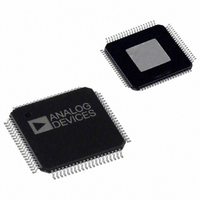
AD9410BSVZ Analog Devices Inc, AD9410BSVZ Datasheet - Page 17

AD9410BSVZ
Manufacturer Part Number
AD9410BSVZ
Description
10 BIT 210 MSPS ADC
Manufacturer
Analog Devices Inc
Datasheet
1.AD9410BSVZ.pdf
(20 pages)
Specifications of AD9410BSVZ
Number Of Bits
10
Sampling Rate (per Second)
210M
Data Interface
Parallel
Number Of Converters
1
Power Dissipation (max)
2.4W
Voltage Supply Source
Analog and Digital
Operating Temperature
-40°C ~ 85°C
Mounting Type
Surface Mount
Package / Case
80-TQFP Exposed Pad, 80-eTQFP, 80-HTQFP, 80-VQFP
Lead Free Status / RoHS Status
Lead free / RoHS Compliant
Available stocks
Company
Part Number
Manufacturer
Quantity
Price
Company:
Part Number:
AD9410BSVZ
Manufacturer:
ADI
Quantity:
115
Company:
Part Number:
AD9410BSVZ
Manufacturer:
Analog Devices Inc
Quantity:
10 000
VOLTAGE REFERENCE
A stable and accurate 2.5 V voltage reference is built into the
AD9410 (VREF
the reference voltage. No appreciable degradation in
performance occurs when the reference is adjusted ±5%. The
full-scale range of the ADC tracks reference voltage changes
linearly within the ±5% tolerance.
TIMING
The AD9410 provides latched data outputs, with six pipeline
delays in interleaved mode (see Figure 2). In parallel mode, the
Port A has one additional cycle of latency added on-chip to line
up transitions at the data ports, resulting in a latency of seven
cycles for the Port A. The length of the output data lines and
loads placed on them should be minimized to reduce transients
within the AD9410; these transients can detract from the
dynamic performance of the converter.
The minimum guaranteed conversion rate of the AD9410 is
100 MSPS. At internal clock rates below 100 MSPS, dynamic
performance may degrade. Note that lower effective sampling
rates can be obtained simply by sampling just one output port—
decimating the output by two. Lower sampling frequencies can
also be accommodated by restricting the duty cycle of the clock
such that the clock high pulse width is a maximum of 5 ns.
OUT
). The input range can be adjusted by varying
Rev. A | Page 17 of 20
DATA SYNC (DS)
The data sync input, DS, can be used in applications requiring
that a given sample appear at a specific output Port A or Port B.
When DS is held high, the ADC data outputs and clock do not
switch and are held static. Synchronization is accomplished by
the assertion (falling edge) of DS, within the timing constraints
t
synchronization, t
required setup time (t
analog value at that point is digitized and available at Port B six
cycles later (interleaved mode). The next sample, N+1, is
sampled by the next rising clock edge and available at Port A six
cycles after that clock edge (interleaved mode). In dual parallel
mode, Port A has a seven cycle latency, and Port B has a six
cycle latency, but data is available at the same time.
SDS
and t
HDS
relative to an clock rising edge. (On initial
HDS
is not relevant.) If DS falls within the
SDS
) before a given clock rising edge N, the
AD9410


