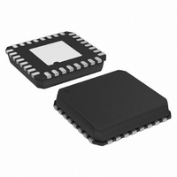
ADN2847ACPZ-32-RL7 Analog Devices Inc, ADN2847ACPZ-32-RL7 Datasheet - Page 11

ADN2847ACPZ-32-RL7
Manufacturer Part Number
ADN2847ACPZ-32-RL7
Description
IC,Laser Diode/LED Driver,LLCC,32PIN,PLASTIC
Manufacturer
Analog Devices Inc
Type
Laser Diode Driver (Fiber Optic)r
Datasheet
1.ADN2847ACPZ-32-RL.pdf
(16 pages)
Specifications of ADN2847ACPZ-32-RL7
Data Rate
3.3Gbps
Number Of Channels
1
Voltage - Supply
3 V ~ 3.6 V
Current - Supply
50mA
Current - Modulation
80mA
Current - Bias
100mA
Operating Temperature
-40°C ~ 85°C
Package / Case
32-VFQFN, CSP Exposed Pad
Mounting Type
Surface Mount
Lead Free Status / RoHS Status
Lead free / RoHS Compliant
ALARM INTERFACES
The FAIL and DEGRADE outputs have an internal pull-up
resistor of 30 kΩ, used to pull the digital high value to V
However, the alarm can be overdriven with an external resistor
allowing alarm interfacing to non-V
output levels must be below the V
POWER CONSUMPTION
The ADN2847 die temperature must be kept below 125°C. Both
LFCSP packages have an exposed paddle that should be connected
in such a manner that is at the same potential as the ADN2847
ground pins. The θ
Absolute Maximum Ratings section. Power consumption can be
calculated using
Thus, the maximum combination of I
calculated, where:
I
I
T
T
V
V
V
LASER DIODE INTERFACING
Many laser diodes designed for 2.5 Gbps operation are packaged
with an internal resistor to bring the effective impedance up to
25 Ω to minimize transmission line effects. In high current
applications, the voltage drop across this resistor combined
with the laser diode forward voltage makes direct connection
between the laser and the driver impractical in a 3 V system.
CCMIN
BIAS
DIE
AMBIENT
BIAS_PIN
MODP_PIN
MODN_PIN
= I
= die temperature
I
P = V
T
Specifications section)
CC
= 50 mA (typical value of I
DIE
MOD
= I
= voltage at I
= ambient temperature
= T
= average voltage at IMODP pin
= average voltage at IMODN pin
CC
CCMIN
= 0
× I
AMBIENT
CC
+ 0.3 I
+ ( I
JA
+ θ
BIAS
BIAS
for both packages is specified in the
JA
MOD
× V
× P
CONTROLLER
pin
BIAS_PIN
AD9850/AD9851
20MHz TO 180MHz
CLKIN
REF CLOCK
AD9834
CC
R
) + I
Figure 12. Application Circuit to Allow Fiber Identification Using the AD9850/AD9851
CC
DDS
SET
provided in the
9
CC
used for the ADN2847.
MOD
BIAS
12
levels. Non-V
37.5µA TO 600µA
( V
+ I
MODP_PIN
20
MOD
21
1.25mA TO 20mA
I
OUT
I
must be
OUT
+ V
50Ω
CC
MODN_PIN
50Ω
alarm
CC
.
(DC-COUPLED)
Rev. A | Page 11 of 16
)/2
LP FILTER
BC550
AC coupling the driver to the laser diode removes this
headroom constraint.
Caution must be taken when choosing component values for
ac coupling (see Figure 15) to ensure that the time constants
(L/R and RC) are sufficiently long for the data rate and expected
number of consecutive identical digits (CIDs). Failure to do this
can lead to pattern dependent jitter and vertical eye closure.
For designs with low series resistance, or where external
components become impractical, the ADN2847 supports direct
connection to the laser diode (see Figure 14). In this case, care
must be taken to ensure that the voltage drop across the laser
diode does not violate the minimum compliance voltage on the
IMODP pin.
OPTICAL SUPERVISOR
The PSET and ERSET potentiometers can be replaced with a
dual-digital potentiometer, the ADN2850 (see Figure 13). The
ADN2850 provides an accurate digital control for the average
optical power and extinction ratio and ensures excellent
stability over temperature.
1.3kΩ
AD8602
AD8602
CLK
1/2
Rx
CS
Tx
1/2
Figure 13. Application Using the ADN2850 a Dual 10-Bit Digital
Potentiometer with an Extremely Low Temperature Coefficient
SDI
SDO
CLK
CS
ADN2850
BC550
10kHz TO 1MHz
50µA TO 800µA
500Ω
V
0.125mA TO 2mA
CC
1kΩ
DAC1
DAC2
as an Optical Supervisor
IDTONE
DATAP
DATAN
PSET
ERSET
35
32
IMPD
V
ADN2847
ADN2847
IMMON
IDTONE
CC
IMODP
I
BIAS
ADN2847
V
CC
V
CC
R
Z


