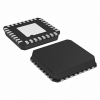
ADN2847ACPZ-32-RL7 Analog Devices Inc, ADN2847ACPZ-32-RL7 Datasheet - Page 9

ADN2847ACPZ-32-RL7
Manufacturer Part Number
ADN2847ACPZ-32-RL7
Description
IC,Laser Diode/LED Driver,LLCC,32PIN,PLASTIC
Manufacturer
Analog Devices Inc
Type
Laser Diode Driver (Fiber Optic)r
Datasheet
1.ADN2847ACPZ-32-RL.pdf
(16 pages)
Specifications of ADN2847ACPZ-32-RL7
Data Rate
3.3Gbps
Number Of Channels
1
Voltage - Supply
3 V ~ 3.6 V
Current - Supply
50mA
Current - Modulation
80mA
Current - Bias
100mA
Operating Temperature
-40°C ~ 85°C
Package / Case
32-VFQFN, CSP Exposed Pad
Mounting Type
Surface Mount
Lead Free Status / RoHS Status
Lead free / RoHS Compliant
THEORY OF OPERATION
Laser diodes have current-in to light-out transfer functions, as
shown in Figure 9. Two key characteristics of this transfer
function are the threshold current, I
linear region beyond the threshold current, referred to as slope
efficiency (LI).
CONTROL
A monitor photodiode (MPD) is required to control the LD. The
MPD current is fed into the ADN2847 to control the power and
extinction ratio, continuously adjusting the bias current and
modulation current in response to the changing threshold
current and light-to-current slope efficiency of the laser.
The ADN2847 uses automatic power control (APC) to maintain
a constant average power over time and temperature.
The ADN2847 uses closed-loop extinction ratio control to allow
optimum setting of the extinction ratio for every device. Thus,
SONET/SDH interface standards can be met over device variation,
temperature, and laser aging. Closed-loop modulation control
eliminates the need to either overmodulate the LD or include
external components for temperature compensation. This
reduces research and development time and second sourcing
issues caused by characterizing LDs.
Average power and extinction ratio are set using the PSET pin
and the ERSET pin, respectively. Potentiometers are connected
between these pins and ground. The potentiometer R
to change the average power. The potentiometer R
to adjust the extinction ratio. Both PSET and ERSET are kept
1.2 V above GND.
The R
following formulas:
R
R
PSET
PSET
ERSET
and R
=
=
1
P
P1
P0
AV
2 .
I
I
ERSET
AV
MPD
V
P
Figure 9. Laser Transfer Function
CW
ER =
P
potentiometers can be calculated using the
_
( )
AV
Ω
CW
=
P1
P0
P1 + P0
1
×
2 .
2
ER
ER
V
−
+
I
1
1
TH
×
TH
ΔI
P
, and the slope in the
AV
CURRENT
ΔP
( )
LI =
Ω
ΔP
ΔI
ERSET
PSET
is used
is used
Rev. A | Page 9 of 16
where:
I
P
I
P
ER is the desired extinction ratio (ER = P1/P0).
Note that I
the control loops determines actual values. It is not required to
know exact values for LI or MPD optical coupling.
LOOP BANDWIDTH SELECTION
For continuous operation, the user should hardwire the LBWSET
pin high and use 1 μF capacitors to set the actual loop bandwidth.
These capacitors are placed between the PAVCAP pin and the
ERCAP pin and ground. It is important that these capacitors are
low leakage multilayer ceramics with an insulation resistance
greater than 100 GΩ or a time constant of 1000 seconds,
whichever is less.
Table 6.
Operation
Mode
Continuous
50 Mbps to
3.3 Gbps
Optimized for
2.5 Gbps to
3.3 Gbps
Setting LBSET low and using 22 nF capacitors results in a
shorter loop time constant (a 10× reduction over using 1 μF
capacitors and keeping LBWSET high.)
ALARMS
The ADN2847 is designed to allow interface compliance to
ITUT-G958 (11/94) section 10.3.1.1.2 (transmitter fail) and
section 10.3.1.1.3 (transmitter degrade). The ADN2847 has two
active high alarms, DEGRADE and FAIL. A resistor between
ground and the ASET pin is used to set the current at which
these alarms are raised. The current through the ASET resistor
is a ratio of 100:1 to the FAIL alarm threshold. The DEGRADE
alarm is raised at 90% of this level.
Example:
where the smallest valid value for R
corresponds to the I
AV
MPD_CW
CW
AV
is the average MPD current.
is the average power required.
is the dc optical power specified on the laser data sheet.
I
I
R
FAIL
ASET
ASET
is the MPD current at that specified P
=
ERSET
=
=
50
I
1
100
I
FAIL
2 .
ASET
and I
mA
V
LBWSET
High
Low
=
so
=
BIAS
PSET
50
500
100
I
maximum of 100 mA.
DEGRADE
mA
1
changes from device to device; however,
2 .
μA
=
Recommended
PAVCAP
1 μF
22 nF
=
500
=
2
4 .
45
μA
ASET
kΩ
mA
is 1.2 kΩ, because this
CW
.
Recommended
ERCAP
1 μF
22 nF
ADN2847


