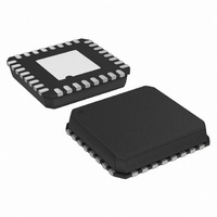
ADN2847ACPZ-32-RL7 Analog Devices Inc, ADN2847ACPZ-32-RL7 Datasheet - Page 3

ADN2847ACPZ-32-RL7
Manufacturer Part Number
ADN2847ACPZ-32-RL7
Description
IC,Laser Diode/LED Driver,LLCC,32PIN,PLASTIC
Manufacturer
Analog Devices Inc
Type
Laser Diode Driver (Fiber Optic)r
Datasheet
1.ADN2847ACPZ-32-RL.pdf
(16 pages)
Specifications of ADN2847ACPZ-32-RL7
Data Rate
3.3Gbps
Number Of Channels
1
Voltage - Supply
3 V ~ 3.6 V
Current - Supply
50mA
Current - Modulation
80mA
Current - Bias
100mA
Operating Temperature
-40°C ~ 85°C
Package / Case
32-VFQFN, CSP Exposed Pad
Mounting Type
Surface Mount
Lead Free Status / RoHS Status
Lead free / RoHS Compliant
SPECIFICATIONS
V
at T
Table 1.
Parameter
LASER BIAS CURRENT (I
MODULATION CURRENT (IMODP, IMODN)
MONITOR PD (MPD, MPD2)
POWER SET INPUT (PSET)
EXTINCTION RATIO SET INPUT (ERSET)
ALARM SET (ASET)
CONTROL LOOP
DATA INPUTS (DATAP, DATAN, CLKP, CLKN)
LOGIC INPUTS (ALS, LBWSET, CLKSEL)
ALARM OUTPUTS (FAIL, DEGRADE)
IDTONE
CC
Output Current I
I
I
CCBIAS Compliance Voltage
Output Current I
Compliance Voltage
I
Rise Time
Fall Time
Random Jitter
Pulse Width Distortion
Current
Compliance Voltage
Capacitance
Monitor Photodiode Current into RPSET Resistor
Voltage
Allowable Resistance Range
Voltage
Allowable Resistance Range
Voltage
Hysteresis
Time Constant
V p-p (Single-Ended, Peak-to-Peak)
Input Impedance (Single-Ended)
t
t
V
V
V
V
Compliance Voltage
f
BIAS
BIAS
MOD
SETUP
HOLD
IN
IH
IL
OH
OL
A
= 3.0 V to 3.6 V. Temperature range: −40°C to +85°C. All specifications T
5
ALS Assertion Time
I
= 25°C.
OUT
when ALS is asserted
Compliance Voltage
when ALS is Asserted
4
4
/I
IN
2
Ratio
2
2
BIAS
MOD
BIAS
2
, ALS)
1
3
Min
2
1.2
1.2
5
1.5
50
1.1
1.2
1.1
1.2
1.1
100
50
100
2.4
2.4
0.01
50
Rev. A | Page 3 of 16
Typ
80
80
1
15
1.2
1.2
1.2
5
0.22
2.25
50
V
2
CC
− 1.5
Max
100
5
V
V
80
V
120
120
1.5
1200
1.65
80
1.3
25
1.3
25
1.3
500
0.8
0.8
1
0.1
0.1
1200
CC
CC
CC
MIN
to T
MAX
Unit
mA
mA
μs
V
V
mA
V
mA
ps
ps
ps
ps
μA
V
pF
μA
V
kΩ
V
kΩ
V
%
sec
sec
mV
Ω
ps
ps
V
V
V
V
V
MHz
, unless otherwise noted. Typical values specified
Internal 30 kΩ Pull-Up
Conditions/Comments
I
See Figure 3 for device rise time histogram
See Figure 4 for device fall time histogram
RMS
I
Average current
Average current
Low Loop Bandwidth selection
LBWSET = GND
LBWSET = V
Data and clock inputs are ac-coupled
See Figure 2
See Figure 2
User to supply current sink in the range of
50 μA to 4 mA
BIAS
MOD
< 10% of nominal
= 40 mA
CC
ADN2847


