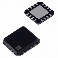
ADN2892ACPZ-RL Analog Devices Inc, ADN2892ACPZ-RL Datasheet - Page 12

ADN2892ACPZ-RL
Manufacturer Part Number
ADN2892ACPZ-RL
Description
IC,Application Specific Amplifier,SINGLE,LLCC,16PIN,PLASTIC
Manufacturer
Analog Devices Inc
Datasheet
1.ADN2892ACPZ-RL.pdf
(16 pages)
Specifications of ADN2892ACPZ-RL
Amplifier Type
Limiting
Number Of Circuits
1
-3db Bandwidth
1.5GHz
Voltage - Input Offset
100µV
Current - Supply
48mA
Voltage - Supply, Single/dual (±)
2.9 V ~ 3.6 V
Operating Temperature
-40°C ~ 95°C
Mounting Type
Surface Mount
Package / Case
16-LFCSP
Lead Free Status / RoHS Status
Lead free / RoHS Compliant
Output Type
-
Current - Output / Channel
-
Slew Rate
-
Gain Bandwidth Product
-
Current - Input Bias
-
Lead Free Status / RoHS Status
Lead free / RoHS Compliant
ADN2892
PCB Layout
Figure 19 shows the recommended PCB layout. The 50 Ω
transmission lines are the traces that bring the high frequency
input and output signals (PIN, NIN, OUTP, and OUTN) from a
terminated source to a terminated load with minimum
reflection. To avoid a signal skew between the differential
traces, each differential PIN/NIN and OUTP/OUTN pair
should have matched trace lengths from a differential source to
a differential load. C1, C2, C3, and C4 are ac coupling
capacitors in series with the high speed, signal input/output
paths. To minimize the possible mismatch, the ac coupling
capacitor pads should be the same width as the 50 Ω
transmission line trace width. To reduce supply noise, a 1 nF
decoupling capacitor should be placed as close as possible to the
VCC pins on the same layer and not through vias. A 0.1 µF
decoupling capacitor can be placed on the bottom of the PCB
directly underneath the 1 nF capacitor. All high speed, CML
outputs have internal 50 Ω resistor termination between the
output pin and VCC. The high speed inputs, PIN and NIN, also
have the internal 50 Ω termination to an internal reference
voltage.
As with any high speed, mixed-signal design, keep all high
speed digital traces away from sensitive analog nodes.
∼
4mm
PIN
NIN
BOTTOM OF BOARD
TO ROSA
UNDERNEATH C6
PLACE C5 ON
C1
C2
GND
VIA TO C12, R2
ON BOTTOM
C6
AVCC
Figure 19. Recommended ADN2892 PCB Layout (Top View)
1
R1, C9, C10 ON BOTTOM
VIAS TO BOTTOM
FILLED VIAS TO
EXPOSED PAD
Rev. 0 | Page 12 of 16
GND
Soldering Guidelines for the LFCSP
The lands on the 16-lead LFCSP are rectangular. The PCB pad
for these should be 0.1 mm longer than the package land length
and 0.05 mm wider than the package land width. The land
should be centered on the pad. This ensures that the solder joint
size is maximized. The bottom of the LFCSP has a central
exposed pad. The pad on the printed circuit board should be at
least as large as the exposed pad. Users must connect the
exposed pad to VEE using filled vias so that solder does not
leak through the vias during reflow. This ensures a solid
connection from the exposed pad to VEE.
PAD COATING AND PB-FREE SOLDERING
Table 5.
Pad Coating
Pb-Free Reflow Portfolio
DVCC GND
DOUBLE-VIA TO GND
TO REDUCE INDUCTANCE
C8
DOUBLE-VIAS TO REDUCE
INDUCTANCE TO SUPPLY
AND GND
PLACE C7 ON
BOTTOM OF BOARD
UNDERNEATH C8
C3
C4
TRANSMISSION LINES SAME
WIDTH AS AC COUPLING
CAPS TO REDUCE REFLECTIONS
OUTP
OUTN
Matt-Tin
J-STD-20B


