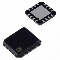
ADN2892ACPZ-RL Analog Devices Inc, ADN2892ACPZ-RL Datasheet - Page 3

ADN2892ACPZ-RL
Manufacturer Part Number
ADN2892ACPZ-RL
Description
IC,Application Specific Amplifier,SINGLE,LLCC,16PIN,PLASTIC
Manufacturer
Analog Devices Inc
Datasheet
1.ADN2892ACPZ-RL.pdf
(16 pages)
Specifications of ADN2892ACPZ-RL
Amplifier Type
Limiting
Number Of Circuits
1
-3db Bandwidth
1.5GHz
Voltage - Input Offset
100µV
Current - Supply
48mA
Voltage - Supply, Single/dual (±)
2.9 V ~ 3.6 V
Operating Temperature
-40°C ~ 95°C
Mounting Type
Surface Mount
Package / Case
16-LFCSP
Lead Free Status / RoHS Status
Lead free / RoHS Compliant
Output Type
-
Current - Output / Channel
-
Slew Rate
-
Gain Bandwidth Product
-
Current - Input Bias
-
Lead Free Status / RoHS Status
Lead free / RoHS Compliant
SPECIFICATIONS
Test Conditions: VCC = 2.9 V to 3.6 V, VEE = 0 V, T
Table 1.
Parameter
QUANTIZER DC CHARACTERISTICS
QUANTIZER AC CHARACTERISTICS
LOSS OF SIGNAL DETECTOR (LOS)
RSSI
BW_SEL (BANDWIDTH SELECTION)
POWER SUPPLIES
OPERATING TEMPERATURE RANGE
CML OUTPUT CHARACTERISTICS
Input Voltage Range
Input Common Mode
Peak-to-Peak Differential Input Range
Input Sensitivity
Input Offset Voltage
Input RMS Noise
Input Resistance
Input Capacitance
Input Data Rate
Small Signal Gain
S11
S22
Random Jitter
Deterministic Jitter
Low Frequency Cutoff
Power Supply Rejection
LOS Assert Level
Electrical Hysteresis
LOS Assert Time
LOS Deassert Time
Input Current Range
RSSI Output Linearity
Gain
Offset
Compliance Voltage (At PD_CATHODE)
Channel Bandwidth
V
I
Output Impedance
Output Voltage Swing
Output Rise and Fall Time
CC
CC
Min
V
2.1
6.6
1.0
2.9
22.4
2.5
2.8
5
V
V
2.9
−40
600
CC
CC
CC
A
− 1.2
− 0.4
− 0.9
= −40°C to +95°C, unless otherwise noted.
Rev. 0 | Page 3 of 16
Typ
3.5
100
235
50
0.65
51
−10
−10
3.0
10
30
45
3.5
35
5.0
5.0
950
62
2
1.0
145
1.5
3.3
48
+25
50
750
70
Max
V
2.7
2.0
4.25
3.9
21.0
4.8
55.0
1000
3.6
54
+95
940
103
CC
− 0.2
kHz
V p-p
Unit
V
V
V p-p
mV p-p
µV
µV rms
Ω
pF
Gbps
dB
dB
dB
ps rms
ps p-p
dB
mV p-p
mV p-p
dB
dB
ns
ns
µA
%
mA/mA
nA
V
V
GHz
V
mA
°C
Ω
ps
Test Conditions/Comments
At PIN or NIN, dc-coupled
DC-coupled
PIN − NIN, ac-coupled
PIN − NIN, BER ≤ 1 × 10
Single-ended
Differential
Differential, f < 4.25 GHz
Differential, f < 4.25 GHz
Input ≥ 10 mV p-p, 4× FC, K28.7 pattern
Input ≥ 10 mV p-p, 4× FC, K28.5 pattern
100 kHz < f < 10 MHz
R
R
1.0 Gbps, PRBS 2
4× FC, PRBS 2
DC-coupled
DC-coupled
5 µA ≤ I
I
I
I
−3 dB cutoff frequency of the on-chip,
two-pole, low-pass filter, when BW_SEL = 0
T
Single-ended
Differential
20% to 80%
RSSI
PD_CATHODE
PD_CATHODE
MIN
THRADJ
THRADJ
/I
to T
PD_CATHODE
= 100 kΩ
= 1 kΩ
IN
MAX
≤ 1000 µA
= 5 µA
= 1000 µA
23
− 1
23
− 1
−10
ADN2892


