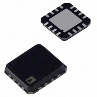
ADN2892ACPZ-RL Analog Devices Inc, ADN2892ACPZ-RL Datasheet - Page 6

ADN2892ACPZ-RL
Manufacturer Part Number
ADN2892ACPZ-RL
Description
IC,Application Specific Amplifier,SINGLE,LLCC,16PIN,PLASTIC
Manufacturer
Analog Devices Inc
Datasheet
1.ADN2892ACPZ-RL.pdf
(16 pages)
Specifications of ADN2892ACPZ-RL
Amplifier Type
Limiting
Number Of Circuits
1
-3db Bandwidth
1.5GHz
Voltage - Input Offset
100µV
Current - Supply
48mA
Voltage - Supply, Single/dual (±)
2.9 V ~ 3.6 V
Operating Temperature
-40°C ~ 95°C
Mounting Type
Surface Mount
Package / Case
16-LFCSP
Lead Free Status / RoHS Status
Lead free / RoHS Compliant
Output Type
-
Current - Output / Channel
-
Slew Rate
-
Gain Bandwidth Product
-
Current - Input Bias
-
Lead Free Status / RoHS Status
Lead free / RoHS Compliant
ADN2892
PIN CONFIGURATION AND FUNCTION DESCRIPTIONS
Note that there is an exposed pad on the bottom of the package that must be connected to the GND plane with filled vias.
Table 4. Pin Function Descriptions
Pin No.
1
2
3
4
5
6
7
8
9
10
11
12
13
14
15
16
Exposed Pad
1
P = power; DI = digital input; DO = digital output; AI = analog input; and AO = analog output.
Mnemonic
AVCC
PIN
NIN
AVEE
THRADJ
BW_SEL
LOS_INV
LOS
DRVEE
OUTN
OUTP
DRVCC
SQUELCH
RSSI_OUT
PD_VCC
PD_CATHODE
Pad
I/O Type
P
AI
AI
P
AO
DI
DI
DO
P
DO
DO
P
DI
AO
P
AO
P
1
Description
Analog Power Supply.
Differential Data Input, Positive Port, 50 Ω On-Chip Termination.
Differential Data Input, Negative Port, 50 Ω On-Chip Termination.
Analog Ground.
LOS Threshold Adjust Resistor.
With one 100 kΩ on-chip, pull-up resistor, BW_SEL = 0 for 1×/2× FC, BW_SEL = 1 for 4× FC.
With one 100 kΩ on-chip, pull-down resistor, LOS_INV = 1 inverts the LOS output
to be active low for SFF.
LOS Detector Output, Open Collector.
Output Buffer Ground.
Differential Data Output, CML, Negative Port, 50 Ω, On-Chip Termination.
Differential Data Output, CML, Positive Port, 50 Ω, On-Chip Termination.
Output Buffer Power Supply.
Disable Outputs, 100 kΩ On-Chip, Pull-Down Resistor.
Average Current Output.
Power Input for RSSI Measurement.
Photodiode Bias Voltage.
Connect to Ground.
AVCC
AVEE
NIN
PIN
Figure 2. Pin Configuration
1
2
3
4
Rev. 0 | Page 6 of 16
16
(Not to Scale)
5
ADN2892
TOP VIEW
15
6
14
7
13
8
12
10
11
9
DRVCC
OUTP
OUTN
DRVEE


