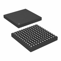
ADSP-2191MKCAZ-160 Analog Devices Inc, ADSP-2191MKCAZ-160 Datasheet - Page 41

ADSP-2191MKCAZ-160
Manufacturer Part Number
ADSP-2191MKCAZ-160
Description
16-bit,160 MIPS, 2.5V,160K Bytes RAM
Manufacturer
Analog Devices Inc
Series
ADSP-21xxr
Type
Fixed Pointr
Datasheet
1.ADSP-2191MKSTZ-160.pdf
(48 pages)
Specifications of ADSP-2191MKCAZ-160
Interface
Host Interface, SPI, SSP, UART
Clock Rate
160MHz
Non-volatile Memory
External
On-chip Ram
160kB
Voltage - I/o
3.00V, 3.30V
Voltage - Core
2.50V
Operating Temperature
0°C ~ 70°C
Mounting Type
Surface Mount
Package / Case
144-MBGA, 144-Mini-BGA
Lead Free Status / RoHS Status
Lead free / RoHS Compliant
Available stocks
Company
Part Number
Manufacturer
Quantity
Price
Company:
Part Number:
ADSP-2191MKCAZ-160
Manufacturer:
ADI
Quantity:
166
Company:
Part Number:
ADSP-2191MKCAZ-160
Manufacturer:
Analog Devices Inc
Quantity:
10 000
The output disable time t
and t
interval from when the reference signal switches to when the
output voltage decays –V from the measured output high or
output low voltage. The t
and I
Output Enable Time
Output pins are considered to be enabled when they have made
a transition from a high impedance state to when they start
driving. The output enable time t
reference signal reaches a high or low voltage level to when the
REV. A
DECAY
L
Figure 27. Equivalent Device Loading for AC
Measurements (Includes All Fixtures)
Figure 28. Voltage Reference Levels for AC
Measurements (Except Output Enable/Disable)
, and with –V equal to 0.5 V.
REFERENCE
V
V
OH (MEASURED)
OL (MEASURED)
O UTPUT
INPUT
as shown in
SIGNAL
OUTPUT
OR
Figure 26. Output Enable/Disable
PIN
TO
t
DIS
OUTPUT STOPS
50pF
DRIVING
t
Figure
DECAY
1.5V
DIS
DECAY
t
TEST CONDITIONS CAUSE THIS VOLTAGE
MEASURED
is the difference between t
V
V
t
26. The time t
DECAY
OH (MEASURED)
OL (MEASURED)
is calculated with test loads C
=
TO BE APPROXIMATELY 1.5V
ENA
HIGH IMPEDANCE STATE.
I
I
OL
C
---------------
OH
L
I
is the interval from when a
L
∆
V
+ V 1.0V
– V 2.0V
1.5V
MEASURED
OUTPUT STARTS
1.5V
t
ENA
DRIVING
MEASURED
is the
L
–41–
output has reached a specified high or low trip point, as shown
in the Output Enable/Disable diagram
pins (such as the data bus) are enabled, the measurement value
is that of the first pin to start driving.
Example System Hold Time Calculation
To determine the data output hold time in a particular system,
first calculate t
on Page
ADSP-2191M’s output voltage and the input threshold for the
device requiring the hold time. A typical –V will be 0.4 V. C
the total bus capacitance (per data line), and I
or three-state current (per data line). The hold time will be t
plus the minimum disable time (i.e., t
write cycle).
Capacitive Loading
Output delays and holds are based on standard capacitive loads:
50 pF on all pins (see
tions given should be derated by a factor of 1.5 ns/50 pF for loads
other than the nominal value of 50 pF.
show how output rise time varies with capacitance. These figures
also show graphically how output delays and holds vary with load
capacitance. (Note that this graph or derating does not apply to
output disable delays; see
graphs in these figures may not be linear outside the ranges
shown.
Environmental Conditions
The thermal characteristics in which the DSP is operating
influence performance.
Thermal Characteristics
The ADSP-2191M comes in a 144-lead LQFP or 144-lead Ball
Grid Array (mini-BGA) package. The ADSP-2191M is specified
for an ambient temperature (T
formula below.
Figure 29. Typical Output Rise Time (10%-90%,
V
Temperature) vs. Load Capacitance
DDEXT
40
30
20
10
40. Choose –V to be the difference between the
0
0
= Minimum at Maximum Ambient Operating
DECAY
50
using the equation at
Figure
LOAD CAPACITANCE – pF
Output Disable Time on Page
100
30). The delay and hold specifica-
AMB
RISE TIME
) as calculated using the
ADSP-2191M
DATRWH
150
Figure 28
(Figure
Output Disable Time
FALL TIME
L
for the
is the total leakage
26). If multiple
200
and
Figure 29
40.) The
250
DECAY
L
is


