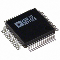
ADUC836BSZ Analog Devices Inc, ADUC836BSZ Datasheet - Page 15

ADUC836BSZ
Manufacturer Part Number
ADUC836BSZ
Description
16bit Dual ADC With Embedded 8 Bit MCU
Manufacturer
Analog Devices Inc
Series
MicroConverter® ADuC8xxr
Datasheet
1.ADUC836BSZ.pdf
(80 pages)
Specifications of ADUC836BSZ
Core Processor
8052
Core Size
8-Bit
Speed
12.58MHz
Connectivity
EBI/EMI, I²C, SPI, UART/USART
Peripherals
POR, PSM, PWM, Temp Sensor, WDT
Number Of I /o
34
Program Memory Size
62KB (62K x 8)
Program Memory Type
FLASH
Eeprom Size
4K x 8
Ram Size
2.25K x 8
Voltage - Supply (vcc/vdd)
2.7 V ~ 5.25 V
Data Converters
A/D 7x16b; D/A 1x12b
Oscillator Type
Internal
Operating Temperature
-40°C ~ 125°C
Package / Case
52-MQFP, 52-PQFP
Cpu Family
ADuC8xx
Device Core
8052
Device Core Size
8b
Frequency (max)
12.58MHz
Interface Type
I2C/SPI/UART
Total Internal Ram Size
2.25KB
# I/os (max)
26
Number Of Timers - General Purpose
3
Operating Supply Voltage (typ)
3.3/5V
Operating Supply Voltage (max)
5.25V
Operating Supply Voltage (min)
2.7V
On-chip Adc
2(2-chx16-bit)
On-chip Dac
1-chx12-bit
Instruction Set Architecture
CISC
Operating Temp Range
-40C to 125C
Operating Temperature Classification
Automotive
Mounting
Surface Mount
Pin Count
52
Package Type
MQFP
Package
52MQFP
Family Name
ADuC8xx
Maximum Speed
12.58 MHz
Operating Supply Voltage
3.3|5 V
Data Bus Width
8 Bit
Number Of Programmable I/os
26
Number Of Timers
3
Lead Free Status / RoHS Status
Lead free / RoHS Compliant
Lead Free Status / RoHS Status
Lead free / RoHS Compliant
Available stocks
Company
Part Number
Manufacturer
Quantity
Price
Company:
Part Number:
ADUC836BSZ
Manufacturer:
ADI
Quantity:
150
Company:
Part Number:
ADUC836BSZ
Manufacturer:
Analog Devices Inc
Quantity:
10 000
Part Number:
ADUC836BSZ
Manufacturer:
ADI/亚德诺
Quantity:
20 000
Stack Pointer (SP and SPH)
The SP SFR is the stack pointer and is used to hold an internal
RAM address that is called the “top of the stack.”The SP Register
is incremented before data is stored, during PUSH and CALL
executions.While the Stack may reside anywhere in on-chip RAM,
the SP Register is initialized to 07H after a reset. This causes the
stack to begin at location 08H.
As mentioned earlier, the ADuC836 offers an extended 11-bit
stack pointer. The three extra bits that make up the 11-bit stack
pointer are the 3 LSBs of the SPH byte located at B7H.
Program Status Word (PSW)
The PSW SFR contains several bits reflecting the current status
of the CPU as detailed in Table I.
SFR Address
Power-On Default Value
Bit Addressable
Bit
7
6
5
4
3
2
1
0
Power Control SFR (PCON)
The PCON SFR contains bits for power saving options and
general-purpose status flags, as shown in Table II.
The TIC (Wake-Up/RTC timer) can be used to accurately wake
up the ADuC836 from power-down at regular intervals. To use
the TIC to wake up the ADuC836 from power-down, the OSC_PD
bit in the PLLCON SFR must be clear and the TIC must be
enabled.
SFR Address
Power-On Default Value
Bit Addressable
REV. A
AC
Table I. PSW SFR Bit Designations
Name
CY
F0
RS1
RS0
OV
F1
P
Description
Carry Flag
Auxiliary Carry Flag
General-Purpose Flag
Register Bank Select Bits
RS1
0
0
1
1
Overflow Flag
General-Purpose Flag
Parity Bit
D0H
00H
Yes
87H
00H
No
RS0
0
1
0
1
Selected Bank
0
1
2
3
–15–
Bit
7
6
5
4
3
2
1
0
ADuC836 CONFIGURATION SFR (CFG836)
The CFG836 SFR contains the necessary bits to configure the
internal XRAM and the extended SP. By default it configures
the user into 8051 mode, i.e., extended SP is disabled, internal
XRAM is disabled.
SFR Address
Power-On Default Value
Bit Addressable
Bit
7
6
5
4
3
2
1
0
Name
EXSP
–––
–––
–––
–––
–––
–––
XRAMEN XRAM Enable Bit. If this bit is set, the in-
ALEOFF
Name
SMOD
SERIPD
INT0PD
GF1
GF0
PD
IDL
Table III. CFG836 SFR Bit Designations
Table II. PCON SFR Bit Designations
Description
Extended SP Enable. If this bit is set, the
stack will roll over from SPH/SP = 00FFH to
0100H. If this bit is clear, the SPH SFR will
be disabled and the stack will roll over from
SP = FFH to SP = 00H.
Reserved for Future Use
Reserved for Future Use
Reserved for Future Use
Reserved for Future Use
Reserved for Future Use
Reserved for Future Use
ternal XRAM will be mapped into the lower
2 Kbytes of the external address space. If this
bit is clear, the internal XRAM will not be
accessible and the external data memory will
be mapped into the lower 2 Kbytes of external
data memory (see Figure 3).
Description
Double UART Baud Rate
SPI Power-Down Interrupt Enable
INT0 Power-Down Interrupt Enable
Disable ALE Output
General-Purpose Flag Bit
General-Purpose Flag Bit
Power-Down Mode Enable
Idle Mode Enable
AFH
00H
No
ADuC836


