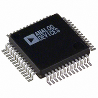
ADUC836BSZ Analog Devices Inc, ADUC836BSZ Datasheet - Page 6

ADUC836BSZ
Manufacturer Part Number
ADUC836BSZ
Description
16bit Dual ADC With Embedded 8 Bit MCU
Manufacturer
Analog Devices Inc
Series
MicroConverter® ADuC8xxr
Datasheet
1.ADUC836BSZ.pdf
(80 pages)
Specifications of ADUC836BSZ
Core Processor
8052
Core Size
8-Bit
Speed
12.58MHz
Connectivity
EBI/EMI, I²C, SPI, UART/USART
Peripherals
POR, PSM, PWM, Temp Sensor, WDT
Number Of I /o
34
Program Memory Size
62KB (62K x 8)
Program Memory Type
FLASH
Eeprom Size
4K x 8
Ram Size
2.25K x 8
Voltage - Supply (vcc/vdd)
2.7 V ~ 5.25 V
Data Converters
A/D 7x16b; D/A 1x12b
Oscillator Type
Internal
Operating Temperature
-40°C ~ 125°C
Package / Case
52-MQFP, 52-PQFP
Cpu Family
ADuC8xx
Device Core
8052
Device Core Size
8b
Frequency (max)
12.58MHz
Interface Type
I2C/SPI/UART
Total Internal Ram Size
2.25KB
# I/os (max)
26
Number Of Timers - General Purpose
3
Operating Supply Voltage (typ)
3.3/5V
Operating Supply Voltage (max)
5.25V
Operating Supply Voltage (min)
2.7V
On-chip Adc
2(2-chx16-bit)
On-chip Dac
1-chx12-bit
Instruction Set Architecture
CISC
Operating Temp Range
-40C to 125C
Operating Temperature Classification
Automotive
Mounting
Surface Mount
Pin Count
52
Package Type
MQFP
Package
52MQFP
Family Name
ADuC8xx
Maximum Speed
12.58 MHz
Operating Supply Voltage
3.3|5 V
Data Bus Width
8 Bit
Number Of Programmable I/os
26
Number Of Timers
3
Lead Free Status / RoHS Status
Lead free / RoHS Compliant
Lead Free Status / RoHS Status
Lead free / RoHS Compliant
Available stocks
Company
Part Number
Manufacturer
Quantity
Price
Company:
Part Number:
ADUC836BSZ
Manufacturer:
ADI
Quantity:
150
Company:
Part Number:
ADUC836BSZ
Manufacturer:
Analog Devices Inc
Quantity:
10 000
Part Number:
ADUC836BSZ
Manufacturer:
ADI/亚德诺
Quantity:
20 000
ADuC836
SPECIFICATIONS
Parameter
LOGIC OUTPUTS (Not Including XTAL2)
POWER SUPPLY MONITOR (PSM)
WATCHDOG TIMER (WDT)
MCU CORE CLOCK RATE
START-UP TIME
FLASH/EE MEMORY RELIABILITY CHARACTERISTICS
V
V
Timeout Period
AV
AV
At Power-On
After External RESET in Normal Mode
After WDT Reset in Normal Mode
Floating State Leakage Current
Floating State Output Capacitance
DV
DV
MCU Clock Rate
From Idle Mode
From Power-Down Mode
Endurance
Data Retention
OH
OL
Oscillator Running
Oscillator Powered Down
DD
DD
DD
DD
, Output Low Voltage
, Output High Voltage
Wake-Up with INT0 Interrupt
Wake-Up with SPI Interrupt
Wake-Up with TIC Interrupt
Wake-Up with External RESET
Wake-Up with INT0 Interrupt
Wake-Up with SPI Interrupt
Wake-Up with External RESET
Trip Point Selection Range
Power Supply Trip Point Accuracy
Trip Point Selection Range
Power Supply Trip Point Accuracy
16
17
2
14
(continued)
2
2
ADuC836
2.4
2.4
0.4
0.4
0.4
±10
5
2.63
4.63
±3.0
±4.0
2.63
4.63
±3.0
±4.0
0
2000
98.3
12.58
300
3
3
10
20
20
20
3
20
20
5
100,000
100
15
–6–
Test Conditions/Comments
V
V
I
I
I
Four Trip Points Selectable in This Range
Programmed via TPA1–0 in PSMCON
T
T
Four Trip Points Selectable in This Range
Programmed via TPD1–0 in PSMCON
T
T
Nine Timeout Periods in This Range
Programmed via PRE3–0 in WDCON
Clock Rate Generated via On-Chip PLL
Programmable via CD2–0 Bits in
PLLCON SFR
Controlled via WDCON SFR
OSC_PD Bit = 0 in PLLCON SFR
OSC_PD Bit = 1 in PLLCON SFR
SINK
SINK
SINK
DD
DD
MAX
MAX
MAX
MAX
= 5 V, I
= 3 V, I
= 8 mA, SCLOCK, MOSI/SDATA
= 10 mA, P1.0 and P1.1
= 1.6 mA, All Other Outputs
= 85°C
= 125°C
= 85C
= 125C
SOURCE
SOURCE
= 80 A
= 20 A
Unit
V min
V min
V max
V max
V max
A max
pF typ
V min
V max
% max
% max
V min
V max
% max
% max
ms min
ms max
kHz min
MHz max
ms typ
ms typ
ms typ
s typ
s typ
s typ
s typ
ms typ
s typ
s typ
ms typ
Cycles min
Years min
REV. A


